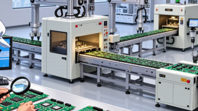
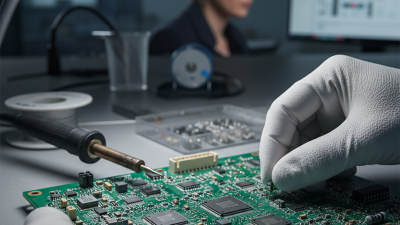
PCB manufacturing and assembly converts an electrical design into a tested, dependable physical product. It includes material selection, circuit imaging, copper etching, drilling, plating, solder-mask application, component placement, soldering, inspection, and final testing. The process looks linear on paper. Production rarely feels that simple.
IPC’s PCB Industry Results reports track sales, orders, and market conditions across major regions. Prismark’s 2024 PCB Industry Forecast examines global production value, regional capacity, and technology demand. These reports show an industry shaped by smartphones, vehicles, medical devices, data centers, and industrial controls. They also reveal pressure from shorter product cycles, tighter trace widths, higher layer counts, and supply-chain uncertainty.
Small details matter.
A few microns of registration error can affect impedance. A poorly controlled reflow profile can weaken a solder joint. Moisture, contamination, or an unsuitable laminate may create failures months later. John W. Mitchell, former IPC President and CEO, described the wider importance clearly: “The electronics industry is the backbone of the global economy, and IPC is the backbone of the electronics industry.” His statement supports a practical view of PCB production: manufacturing quality is not merely a factory concern. It influences safety, reliability, repair costs, and user trust.
This guide will examine each stage, from bare-board fabrication to automated assembly and inspection. It will also question common assumptions. Passing a visual inspection is not enough. A lower purchase price may hide expensive field failures. The strongest process balances engineering evidence, supplier capability, traceability, and honest risk assessment.
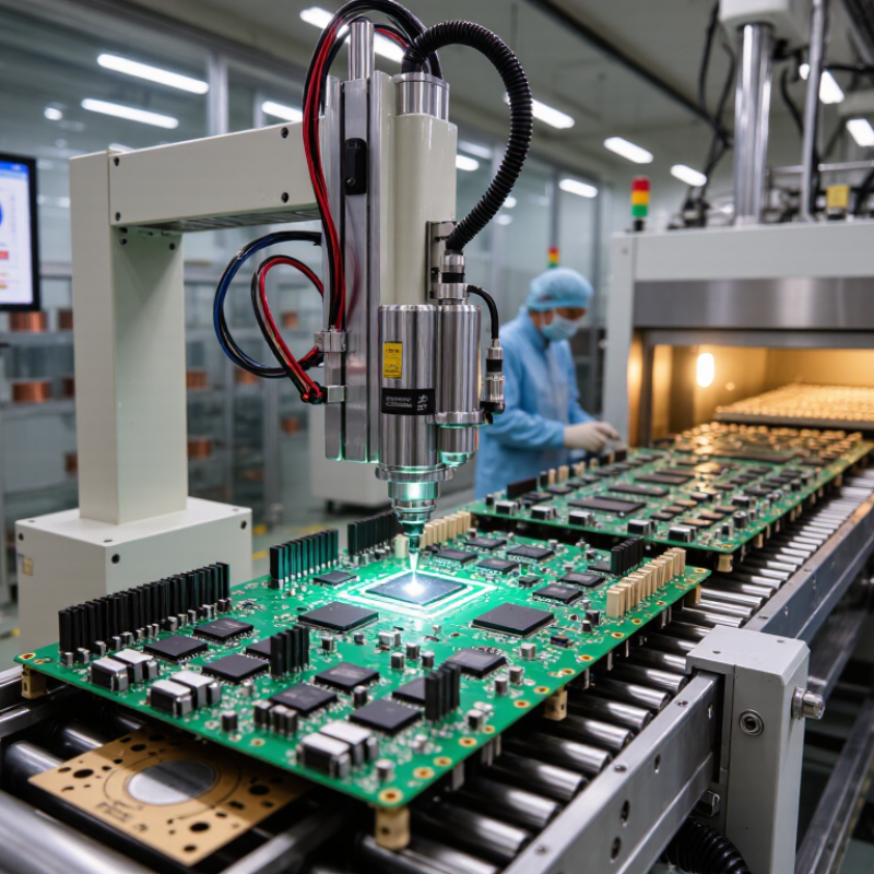
What Is PCB Manufacturing and Assembly?
PCB manufacturing and assembly involve turning a circuit design into a tested electronic board. Manufacturing creates the bare board, while assembly adds components and prepares it for operation.
Manufacturing starts with copper-clad laminate. Engineers transfer the circuit pattern onto copper layers, then etch away unwanted areas. Drilling creates holes for connections between layers. Plating strengthens these holes and improves electrical continuity. Solder mask protects exposed copper from oxidation and accidental shorts. Printed markings identify component locations during assembly. Each layer needs careful alignment. Even a small registration error can affect signal paths or create an unusable board.
Assembly begins with solder paste applied through a metal stencil. Automated equipment places resistors, capacitors, and integrated circuits onto the paste. A controlled reflow oven melts the solder and forms permanent joints. Larger or irregular parts may require manual placement or through-hole soldering. Technicians then inspect the board using magnification, optical systems, or X-ray inspection. Functional testing checks whether power, signals, and interfaces behave correctly. It catches problems that visual inspection cannot.
No process is flawless. A practical lesson is that clean design data matters as much as modern equipment. Incorrect footprints, unclear tolerances, or missing test points can delay production. Engineers should review manufacturability before ordering boards. They also need to consider heat, vibration, moisture, and repair access. A board may look perfect under inspection yet fail during real operation. That assumption deserves another test.
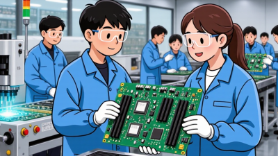
PCB manufacturing converts a circuit design into a physical board through material preparation, lamination, imaging, etching, drilling, plating, and surface finishing. PCB assembly then places electronic components on the finished board and bonds them by soldering.
Chart explanation: Copper foil thickness is commonly specified in ounces per square foot. The nominal conversion is approximately 35 micrometers for each ounce of copper. Thicker copper supports higher current capacity but can require different etching and assembly process controls.
A PCB design becomes production-ready when it survives more than a schematic review. It must fit manufacturing limits, assembly equipment, testing methods, and real operating conditions. Engineers inspect trace widths, copper spacing, hole sizes, layer alignment, and board thickness. They also confirm that components remain available during the expected production period. A beautiful layout can still fail on a factory floor.
Design for manufacturability is practical, not theoretical. A qualified engineer may adjust a crowded connector area, add test points, or increase clearance around heat-producing parts. The fabrication drawing should define materials, surface finish, tolerances, and controlled dimensions. Assembly files must match the final bill of materials. Even a small mismatch can delay production.
That detail matters. During a pilot build, technicians inspect solder joints, component polarity, and paste coverage. Automated optical inspection can reveal shifted parts, but it cannot replace engineering judgment. Functional testing should reflect the product’s actual use, including power-up behavior and communication signals. I have seen prototype boards pass basic checks yet require layout changes after thermal testing. That is not failure; it is useful evidence. Production readiness often improves through careful correction, not perfect planning.ેણ
PCB fabrication turns a digital circuit design into a tested physical board. The process begins with schematic review, layout verification, and Gerber data preparation. Engineers check trace spacing, impedance, hole sizes, and copper thickness. These details prevent expensive rework later.
A manufacturer then presses copper foil onto insulating laminate. Imaging transfers the circuit pattern onto the copper surface. Chemical etching removes unwanted copper, while drilling creates vias and component holes. Plating strengthens these holes and connects multiple layers. Solder mask protects exposed copper, and silkscreen adds reference markings. Surface finishing improves solderability. Electrical testing checks continuity and isolation before assembly. During assembly, machines place components, solder paste is reflowed, and automated optical inspection examines joints. IPC process guidance remains widely used for acceptance and quality control. A 2024 Grand View Research assessment valued the global PCB market at about USD 89.7 billion in 2023, showing the scale of this manufacturing chain.
Tips: Keep fabrication notes inside the design file. Confirm stackup details before ordering. Review drill drawings manually. A perfect-looking board can still fail. I have seen small footprint errors create large assembly delays. That weak point deserves attention. IPC industry surveys also continue to identify material costs and skilled-labor shortages as major production concerns. Therefore, engineers should allow realistic tolerances, inspection time, and supplier feedback. Some designs still prioritize compactness too aggressively. Smaller is not always better.
What Is PCB Manufacturing and Assembly?
PCB manufacturing creates the physical board that carries electrical connections. Assembly places electronic components onto that board. The process begins with a circuit design, material selection, and layer planning. Copper traces are formed, drilled, plated, and protected with a solder mask. Each detail affects current flow, heat control, and long-term reliability.
How Electronic Components Are Assembled onto PCBs
Assembly starts with a verified bill of materials and a bare PCB inspection. A stencil applies solder paste to carefully selected pads. Pick-and-place equipment positions resistors, capacitors, processors, and connectors. The board then passes through a controlled reflow oven. Heat melts the paste and creates solder joints. Through-hole parts may require wave soldering or careful manual soldering. Operators inspect alignment, polarity, and solder quality. Automated optical inspection finds visible defects, while electrical testing checks circuit behavior. A clean board can still fail. Tiny voids, poor moisture control, or one reversed diode may cause trouble later.
Tips: Keep component footprints accurate and review assembly drawings before production. Use ESD protection, clear work instructions, and traceable inspection records. Leave enough spacing around tall parts for tools and repair access. Test a small pilot batch before approving larger production. This step may feel slow, but it often reveals unclear instructions and weak assumptions.
| Process Stage | Primary Purpose | Main Materials or Inputs | Typical Manufacturing Data | Quality Check |
|---|---|---|---|---|
| 1. Circuit Design | Defines electrical connections, component footprints, routing, and mechanical dimensions. | Schematic, PCB layout, fabrication files, assembly drawings, and bill of materials. | Layer count, board outline, hole sizes, trace width, spacing, impedance requirements, and component coordinates. | Design-rule checking, electrical-rule checking, and manufacturability review. |
| 2. Material Preparation | Prepares the laminate and conductive copper layers used to form the circuit board. | Copper-clad laminate, prepreg, copper foil, solder mask, and surface-finish materials. | Common rigid boards use glass-reinforced epoxy laminate; copper thickness is commonly specified in ounces per square foot. | Material certification, thickness measurement, visual inspection, and moisture control. |
| 3. Imaging and Etching | Transfers the circuit pattern to the copper and removes unwanted copper. | Photoresist, imaging data, etching chemistry, and copper-clad panels. | Creates conductive traces, pads, copper pours, and reference features according to the layout. | Automated optical inspection, trace-width measurement, spacing verification, and short/open detection. |
| 4. Layer Lamination | Bonds multiple inner layers into a single multilayer PCB. | Inner-layer cores, copper foil, prepreg, heat, and pressure. | The stack-up controls board thickness, dielectric spacing, signal integrity, and mechanical strength. | Layer-registration inspection, thickness measurement, void checks, and cross-section analysis. |
| 5. Drilling and Plating | Creates component holes and vias, then deposits copper to connect conductive layers. | Mechanical or laser drilling, activation chemicals, and electrolytic copper plating. | Hole types may include through-holes, blind vias, and buried vias; plated holes provide vertical electrical paths. | Hole position, diameter, plating thickness, barrel integrity, and continuity testing. |
| 6. Solder Mask and Surface Finish | Protects exposed copper and improves solderability at assembly pads. | Liquid photoimageable solder mask and a selected copper surface finish. | The solder mask covers most copper while leaving pads, test points, and selected contact areas exposed. | Mask registration, coating coverage, pad cleanliness, finish thickness, and solderability testing. |
| 7. Board Profiling | Separates individual boards from production panels and forms the final outline. | Routing tools, scoring equipment, tooling holes, and panelization data. | The finished outline must match the enclosure, mounting holes, connectors, and keep-out areas. | Dimensional inspection, edge-quality inspection, and verification of mounting features. |
| 8. Solder Paste Printing | Deposits controlled amounts of solder paste onto surface-mount pads. | Solder paste, stencil, PCB, and printer alignment data. | Paste volume and position strongly affect joint formation, bridging, insufficient solder, and component placement. | Solder-paste inspection measures paste height, area, volume, and positional offset. |
| 9. Component Placement | Places surface-mount and, when applicable, through-hole components on the PCB. | Resistors, capacitors, integrated circuits, connectors, sensors, and placement coordinates. | Placement depends on component package, polarity, orientation, feeder setup, and board-side requirements. | Vision alignment, component presence, orientation, polarity, and placement accuracy inspection. |
| 10. Reflow Soldering | Melts solder paste to form permanent electrical and mechanical joints. | Populated PCB, solder paste, and a controlled thermal profile. | The profile includes preheat, thermal soak, time above liquidus, peak temperature, and controlled cooling. | Profile verification, solder-joint inspection, and checks for bridging, voiding, opens, and component damage. |
| 11. Through-Hole Assembly | Installs components whose leads pass through drilled holes in the PCB. | Leaded components, solder, insertion equipment, and selective or wave-soldering equipment. | Often used for mechanically stressed parts, connectors, transformers, and components requiring strong anchoring. | Lead insertion, polarity, solder coverage, hole fill, and joint appearance inspection. |
| 12. Inspection and Testing | Confirms that the assembled PCB meets electrical, mechanical, and visual requirements. | Inspection programs, test fixtures, functional test procedures, and product specifications. | Common methods include automated optical inspection, X-ray inspection, in-circuit testing, and functional testing. | Checks for assembly defects, electrical continuity, shorts, incorrect values, firmware operation, and safety requirements. |
| 13. Cleaning and Final Release | Removes process residues when required and prepares the assembly for shipment or system integration. | Approved cleaning process, inspection criteria, protective packaging, and traceability records. | Final condition may include cleanliness level, conformal coating status, labels, revision, and lot traceability. | Final visual inspection, cleanliness verification, documentation review, and packaging inspection. |
PCB manufacturing and assembly depend on disciplined testing, inspection, and quality control. A board can look clean and still fail under heat, vibration, or electrical load. Technicians therefore inspect solder joints, copper traces, drilled holes, and component alignment. Automated optical inspection detects missing parts and solder bridges. X-ray inspection reveals hidden voids beneath area-array packages.
Electrical testing adds another safeguard. Flying-probe systems check open circuits and unwanted connections. In-circuit testing measures selected components and test points. Functional testing then applies realistic power and signals. IPC-A-600 provides visual acceptability criteria, while IPC-6012 defines performance requirements for rigid printed boards. These standards help teams judge evidence consistently, not by personal preference.
Traceability matters when a defect appears months later. Operators should record material lots, machine settings, inspection images, and rework decisions. The 2024 IBM Cost of a Data Breach Report placed the average breach cost at 4.88 million dollars. That figure concerns cybersecurity, but it illustrates the price of weak controls and missing records. Quality data can also expose recurring defects before they become field failures. Yet inspection is not infallible. False calls waste time, and small process changes may escape detection. Human review still deserves attention.