What Is PCB Board Design and How Does It Work?
A printed circuit board is more than a flat surface for mounting components. It is the electrical and mechanical foundation of devices ranging from smart thermostats to industrial controllers. PCB board design turns a circuit diagram into a manufacturable layout, defining component positions, copper paths, layer stackup, and drilling locations. Small choices matter. A narrow trace can overheat, while a poorly placed connector can complicate assembly.
Industry reports help explain why these decisions matter. IPC’s North American PCB Industry Results tracks sector orders and shipments, offering a practical view of manufacturing activity. WSTS’s Autumn 2024 Semiconductor Market Forecast also documented strong growth in semiconductor demand, which increases pressure to build compact, reliable electronics. These reports do not dictate a board layout. They do show the industrial context in which sound design supports performance, cost, and production needs.
The process usually begins with requirements: power levels, signal speeds, board size, environment, and budget. Designers then capture the schematic, choose components, assign footprints, and arrange parts before routing copper traces. Design-rule checks can catch issues such as inadequate spacing or an unsupported drill size. Manufacturers may also review the files before fabrication. The first layout is rarely perfect. That is normal. A careful designer checks trade-offs, revises weak areas, and verifies the board against applicable IPC standards and manufacturer capabilities. Some details still get missed. A useful design process makes those mistakes easier to find before boards reach the assembly line.
What PCB Board Design Means and the Role It Plays
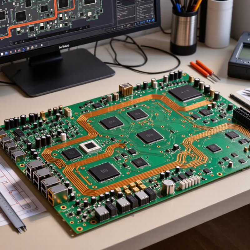
PCB board design turns a circuit diagram into a physical platform for electronic parts and signals. It defines component footprints, copper traces, board layers, vias, and connection points. Think of a phone-sized board: a power trace must carry current, while a nearby signal path may need protection from electrical noise. Small layout choices matter.
The board also connects electrical performance with heat control, assembly, and repair. A designer checks trace width, spacing, and copper thickness, then reviews whether components can be placed and soldered reliably. IPC’s 2022 World PCB Production Report, prepared with Prismark, valued global PCB production at about $81.9 billion. That scale reflects how widely boards support modern electronics, though production value alone cannot measure design quality.
A clean schematic is not enough. A board can pass electrical checks and still be difficult to assemble, or trap heat beneath a component. Design reviews and prototype tests help reveal these gaps. They do not catch everything. Even a small connector shift can complicate a finished product, so designers revisit placement and routing as real manufacturing feedback arrives.
The Main Layers, Components, and Connections on a PCB
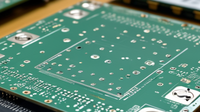
A PCB is more than a flat support for electronic parts. Its layers create both the structure and the electrical paths a circuit needs. A common board has a rigid insulating core, often made from glass-reinforced material, with thin copper layers bonded to it. A solder mask covers most copper, while printed labels identify components and connectors. Simple boards may use two copper layers; complex designs can stack many.
The copper is etched into traces, pads, and larger planes. Traces connect component pins, while vias carry signals between layers through small drilled holes. Power and ground planes provide broad, low-resistance paths. A chip may sit on tiny surface-mount pads, while a larger connector can use plated through-holes. The fit matters. A footprint that is slightly wrong can make assembly difficult.
Design usually begins with a schematic, then moves to a physical layout. Engineers place parts and route connections while checking clearances, current capacity, and signal behavior. A small capacitor placed close to a chip’s power pin can reduce local voltage noise. Fast signals need careful routing, too. A tidy-looking trace is not always electrically sound, and automated checks cannot catch every real-world issue. Prototype measurements may reveal heating, noise, or awkward assembly that the screen did not show. Sometimes the first layout needs revision.
How a PCB Design Is Created Step by Step
PCB design turns an electrical plan into a physical board that connects components reliably. Start by listing what the device must do, its power needs, connectors, and size limits. Then draw a schematic showing how each component connects. Check pin numbers and signal directions carefully; a small schematic error can become a frustrating board revision.
Next, assign each component a footprint that matches its real package. Arrange parts on the board, keeping related components close and allowing room for connectors and mounting holes. Set trace widths and spacing to suit current, voltage, and manufacturing limits. Route the signals, add ground copper if appropriate, and run design-rule checks. Inspect the board in a 3D view, then export manufacturing files. A first prototype may still reveal awkward connector access or noise. That is useful feedback, not failure.
Tips: Place decoupling capacitors close to the power pins they support. Label connectors clearly, and review the layout at actual scale. Ask another engineer to inspect critical connections; fresh eyes often catch what the designer misses.
How PCB Design Files Guide Board Manufacturing
A PCB design file is the handoff between an engineer’s screen and a factory’s machines. It carries more than copper shapes: layer stack-up, hole locations, solder-mask openings, component positions, and manufacturing notes all affect the finished board. Common deliverables include Gerber artwork, drill files, a bill of materials, and pick-and-place coordinates. Formats such as IPC-2581 can bundle design and manufacturing information into one structured exchange. Tiny details matter. A missing drill-plating note, for example, can change how a fabricator builds a via.
Manufacturers use these files to check clearances, plan panels, create tooling, and prepare assembly. They may compare the submitted data against design rules before production; a mismatch can trigger questions or rework. Prismark’s 2023 industry analysis estimated worldwide PCB production value at about US$68.9 billion, showing the scale of an industry where clear data handoffs matter. That figure is market context, not proof that any one file format prevents errors. Engineers still need to review exported layers, units, tolerances, and revision numbers. A rushed export can look complete and still be wrong. I’d treat the file package like a build instruction, not an afterthought: open it, inspect the layer views, and confirm that every document describes the same board.
How PCB Boards Are Tested and Refined for Use
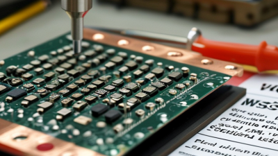
PCB testing starts with the bare board. Technicians inspect copper tracks, drilled holes, solder masks, and board edges for visible defects. Automated optical inspection compares each layer with its design data. It can reveal a narrow trace or a misplaced pad. Small details matter.
Electrical tests check for open circuits and unwanted connections between copper paths. A flying-probe tester suits prototypes and small batches; larger runs may use a fixture with many contact pins. For controlled-impedance boards, measurements can confirm that signal paths meet specified targets. These checks do not prove every board will work in its final device. That takes functional testing after components are installed.
Results guide revisions. A failed connection may call for a wider trace, a better via location, or tighter manufacturing notes. Designers also review test-pad access, component spacing, and heat flow. Reliability checks, such as temperature cycling, may be appropriate for demanding conditions. They can expose weaknesses that a quick bench test misses. Still, testing has limits; a clean report cannot replace careful review of the actual use environment. Feedback from assembly and field trials can reveal awkward details, like a probe blocked by a nearby component, and shape the next board revision.