Why Is PCB Prototyping Important for Product Development?

Why Is PCB Prototyping Important for Product Development?

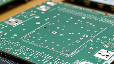
A pcb prototype turns a circuit concept into a physical object that engineers can examine, measure, and improve. Schematics may appear correct on a monitor, yet real boards reveal unexpected problems. A connector may sit too close to an enclosure wall. A trace may run beside a noisy power path. A component may generate more heat than predicted. These details often remain invisible until fabrication and assembly begin.

PCB design educator Robert Feranec captures this practical mindset: “A prototype is the fastest way to discover what you do not know.” A pcb prototype gives development teams evidence before committing to expensive production tooling. Engineers can check signal integrity, power delivery, thermal behavior, soldering quality, and mechanical fit. They can also test firmware with real hardware instead of assumptions. That experience supports more reliable engineering decisions.

Prototypes reduce uncertainty.

They do not remove every risk. A rushed prototype can still hide defects because testing may be incomplete or poorly documented. This is where disciplined review matters. Teams should record test results, inspect solder joints, measure critical signals, and compare performance with design targets. Sometimes, the first board fails. That failure is useful, but only when engineers study its cause. Careful iteration can prevent small prototype issues from becoming costly field failures. In product development, building early is not wasted effort. It is a measurable path toward safer, stronger, and more manufacturable electronics.
Why Is PCB Prototyping Important for Product Development?

What PCB Prototyping Means in Product Development

In product development, PCB prototyping means building a physical version of an electronic design before mass production. It turns a schematic and layout into a board that engineers can touch, power, measure, and revise. The prototype connects design theory with real behavior. It can expose incorrect footprints, noisy signals, weak solder joints, or poor connector placement.

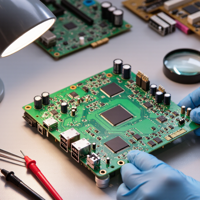
During bench testing, an engineer may use a multimeter and oscilloscope to check voltage, timing, and signal quality. They can inspect hot components with a thermal camera and test the board inside its intended enclosure. A prototype also supports firmware testing because software interacts with actual sensors, buttons, displays, and power circuits. Following recognized engineering and manufacturing practices improves repeatability and safety. Clear revision records make every change traceable.

The first board may not look elegant. That is normal. A connector might be difficult to reach, or a mounting hole may miss its bracket by a few millimeters. These problems are valuable because they appear before expensive production tooling. Testing can still be incomplete if the prototype uses temporary wiring or ideal laboratory power. Engineers should question those assumptions. A second revision often improves routing, heat control, assembly access, and user handling. Each physical board provides evidence that a computer model cannot fully supply.
Why Is PCB Prototyping Important for Product Development?

Prototype validation helps engineering teams identify design issues before production by testing key electrical, thermal, mechanical, and compliance requirements.

Illustrative engineering planning data showing the typical validation coverage enabled by a functional PCB prototype.

How PCB Prototyping Fits into the Product Design Process

PCB prototyping fits between circuit planning and repeatable manufacturing. It turns a schematic into a physical test object. Engineers can inspect routing, connector placement, heat paths, and assembly access before volume production. An early board may reveal a noisy sensor line or a connector blocked by the enclosure. That evidence is more useful than a confident screen review. Keep it practical.

During product design, teams move from requirements to schematic capture, layout, fabrication, assembly, and bench testing. Prototype results then feed back into each stage. Measurements may expose voltage drops, unexpected heating, or weak signal integrity. Engineers can revise trace widths, grounding, component spacing, or firmware assumptions. A thermal camera and oscilloscope often reveal details that calculations miss. I have seen a board pass basic power-up tests yet fail after several hours. That gap deserves attention.

A reliable prototype process records revision numbers, test conditions, failed checks, and design changes. It also separates a quick proof-of-concept from an engineering validation build. The early version may use temporary wiring. A later build should reflect production materials and tolerances. Do not hide awkward findings. A mounting hole shifted by two millimeters can delay assembly and damage confidence. Reviewing such imperfections with manufacturing and quality teams makes decisions more defensible. Prototyping is not a final exam. It is a controlled conversation between design intent and physical behavior.

How Prototype Testing Reveals Design Problems

Why Is PCB Prototyping Important for Product Development?

Prototype testing reveals design problems before they become expensive production failures. A prototype PCB allows engineers to inspect signal behavior, power delivery, thermal performance, and mechanical fit in realistic conditions. A schematic may appear correct, yet a test board can expose unexpected voltage drops or unstable sensor readings.

Small details matter. During testing, engineers can measure current at key points and observe heat near regulators or connectors. They can also check whether cables, enclosures, and mounting holes align properly. These observations provide practical evidence, not assumptions.

Testing should include normal operation, startup, shutdown, vibration, and moderate temperature changes. Engineers often discover issues when several circuits operate at once. For example, a motor may create electrical noise that interrupts a nearby communication line. A poorly placed capacitor may also respond too slowly during a sudden load change.

Not every test result is convenient. Sometimes the prototype needs a complete layout revision. That is useful, although it can feel like lost time. A weak prototype process may focus only on whether the board turns on. That is not enough.

Tips: Record measurements with dates, test conditions, and equipment settings. Photograph unusual marks, damaged components, or loose connections. Invite another engineer to review the test procedure. Fresh eyes can reveal overlooked risks. Leave space for rework, because first prototypes are rarely perfect. Repeating a test is often worthwhile.

Why PCB Prototypes Improve Product Performance and Reliability

Why Is PCB Prototyping Important for Product Development?

Why PCB Prototypes Improve Product Performance and Reliability

A PCB prototype turns a circuit diagram into a working, measurable product. Engineers can inspect signal quality, power delivery, heat behavior, and mechanical fit before production begins. A prototype also reveals practical problems that simulations may miss, such as a connector blocking airflow or a trace running too close to a noisy power section.

Real testing builds reliable evidence. Engineers can measure voltage drops under load, monitor temperature near regulators, and check whether signals remain stable during repeated operation. Small changes, such as widening a copper trace or improving grounding, can reduce interference and prevent early component failure. These improvements often protect performance in ordinary conditions, not only in laboratory tests.

Failure teaches something.

A prototype will not expose every weakness. Environmental stress, assembly variation, and long-term aging may require separate testing. That limitation deserves attention. Still, prototype testing gives development teams a controlled way to compare revisions and record results. I have found that clear test notes are as valuable as the circuit itself. They show why a layout changed, which measurement improved, and where uncertainty remains. This disciplined process supports safer decisions, steadier performance, and more dependable products.

Why Is PCB Prototyping Important for Product Development? - Why PCB Prototypes Improve Product Performance and Reliability

Prototype Stage Primary Validation Objective Key Tests and Measurements Representative Acceptance Criteria Product Performance Benefit Reliability Risk Reduced Outcome
Design Verification Prototype Confirm that the schematic, PCB layout, power distribution, and signal paths operate as intended before production tooling. Electrical continuity, netlist comparison, component polarity, supply-rail voltage, current consumption, and functional tests. 100% of required nets connected; no unintended shorts; supply rails remain within the design tolerance under normal load. Detects incorrect connections, unstable power behavior, and circuit-level design errors early, when changes are less costly. Functional failure, excessive power consumption, incorrect component placement, and intermittent operation. Verified
Signal-Integrity Prototype Validate high-speed signal quality and confirm that the physical stack-up supports the required electrical behavior. Oscilloscope or vector-network measurements of rise time, overshoot, ringing, crosstalk, impedance, and eye-diagram margin. Measured controlled-impedance traces comply with the project specification; signal quality remains within the receiver's voltage and timing limits. Improves data-transfer stability, clock accuracy, electromagnetic compatibility, and system responsiveness. Data corruption, communication dropouts, timing errors, and failures that appear only at higher operating speeds. Validated
Thermal Prototype Determine whether component temperatures and board heat distribution remain acceptable during continuous operation. Thermal-camera or thermocouple measurements, maximum-case temperature, hot-spot location, and temperature rise at rated load. Critical components remain below their specified maximum operating temperatures, with thermal margins maintained at the intended ambient condition. Supports stable performance, prevents thermal throttling, and helps establish heat-sink, copper-area, and enclosure requirements. Premature component aging, solder-joint fatigue, thermal shutdown, and temperature-related drift. Thermally Assessed
Mechanical-Fit Prototype Confirm that the PCB fits the enclosure and aligns correctly with connectors, fasteners, displays, switches, and other mechanical features. Dimensional inspection, hole-position measurement, connector alignment, clearance checks, and enclosure assembly trials. Board outline, mounting holes, keep-outs, and connector locations comply with the mechanical drawing and required clearances. Prevents assembly interference and improves serviceability, connector engagement, and overall product integration. Enclosure damage, connector stress, mounting distortion, vibration-related contact loss, and assembly delays. Fit Confirmed
Manufacturing-Readiness Prototype Evaluate whether the design can be assembled consistently using the intended production process. Design-for-manufacturing review, solder-joint inspection, assembly yield, component accessibility, stencil-aperture review, and rework assessment. All critical features meet the applicable fabrication and assembly requirements; defects are identified, classified, and corrected before volume production. Improves repeatability, reduces assembly variation, and helps control manufacturing cost and production cycle time. Solder bridges, insufficient solder, tombstoning, misplaced parts, hidden defects, and avoidable rework. Production-Ready
Environmental-Stress Prototype Assess whether the PCB maintains operation when exposed to the expected temperature, humidity, vibration, and handling conditions. Temperature cycling, humidity exposure, vibration or shock testing, power cycling, and post-test electrical inspection. No functional failure, unacceptable delamination, cracked solder joints, or electrical degradation after the defined qualification profile. Increases confidence that the product will perform consistently in its intended operating environment. Intermittent faults, corrosion, delamination, solder fatigue, connector loosening, and field returns. Qualified
Compliance Pre-Scan Prototype Identify electromagnetic and electrical safety risks before formal laboratory certification. Radiated-emissions pre-scan, conducted-emissions checks, grounding review, creepage and clearance inspection, and protective-circuit verification. Measured emissions and safety-related construction features meet the applicable product and regulatory requirements defined for the project. Reduces late-stage redesign and improves the probability of passing formal compliance testing. Electromagnetic interference, susceptibility, insulation breakdown, unsafe touch voltage, and certification delays. Pre-Checked
Final Engineering Prototype Confirm that the corrected design performs consistently across representative units before release for production. Functional regression testing, repeated power cycles, dimensional checks, performance comparison, and documented issue closure. All critical requirements pass on the defined sample set, and open design or manufacturing issues have an approved disposition. Provides evidence that design changes solved the original problems without introducing new performance defects. Unresolved design interactions, unit-to-unit variation, latent defects, and unexpected production-line issues. Release Candidate
Reference Framework Use recognized engineering practices to define board design, fabrication, assembly, inspection, and test expectations. Project requirements can reference IPC design and acceptance documents, electrical test procedures, and applicable environmental or safety standards. Requirements are documented, measurable, traceable, and agreed upon before prototype evaluation begins. Creates consistent evaluation criteria and improves communication between design, manufacturing, quality, and test teams. Ambiguous acceptance decisions, undocumented assumptions, inconsistent inspections, and repeated design iterations. Documented

How Prototyping Reduces Development Time, Cost, and Risk

Why Is PCB Prototyping Important for Product Development?

How Prototyping Reduces Development Time, Cost, and Risk

PCB prototyping turns a circuit concept into a board engineers can inspect, test, and improve. A schematic may look correct on screen, but physical spacing can reveal unexpected problems. During testing, a connector may block a mounting hole. A trace may run too close to a noisy power section. These details are easier to fix before full production.

A working prototype also reduces development time and cost. Engineers can measure voltage levels, signal quality, heat, and power consumption with real components. Early tests expose weak assumptions before they become expensive manufacturing changes. Replacing ten boards is usually simpler than correcting thousands. Prototype testing can also support design reviews and provide clear evidence for technical decisions.

Risk becomes more manageable when each revision answers a specific question. Does the board fit the enclosure? Can it survive repeated temperature changes? Will assembly workers reach every component safely? Not every issue appears during the first build. Sometimes, a prototype passes electrical tests but fails after vibration or extended use. That is an uncomfortable result, but it provides useful direction. Careful records of failures, measurements, and design changes help teams avoid repeating the same mistake.

Wordpress Social Share Plugin powered by Ultimatelysocial
Facebook
X (Twitter)
YouTube
LinkedIn
Share

Purchase Product Request

Request Pricing