Top 10 PCB Fabrication Techniques You Should Know?
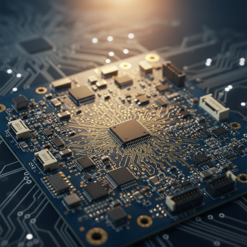
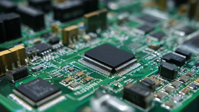
In the world of electronics, PCB fabrication is crucial. Circuit boards are the backbone of modern devices. Without effective techniques, the quality of these boards can suffer.
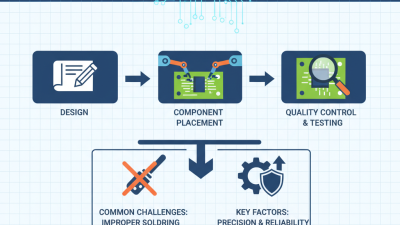
Many people overlook the importance of this process. It's not just about making a board; it's about precision and reliability. Each technique has its strengths and challenges. Some methods are better for complex designs, while others excel in speed and cost.
Understanding different PCB fabrication techniques can transform your projects. The right choice can enhance functionality and performance. As you explore these options, reflect on what methods suit your needs. The goal is to find a balance between quality and efficiency in your PCB fabrication process.
Importance of Choosing the Right PCB Fabrication Technique
Choosing the right PCB fabrication technique impacts the entire electronics manufacturing process. Each method has unique characteristics that affect quality, cost, and efficiency. These factors are critical for successful product development. For example, techniques like etching and laser cutting are widely used, but they have different applications and limitations.
Manufacturers often face challenges when selecting a method. The complexity of the design could require precise specifications. Sometimes, fabricators overlook the importance of alignment or layer stack-up. These oversights can lead to costly defects or delays. Furthermore, understanding material compatibility is crucial. A mismatch can compromise the PCB's durability and performance.
Evaluating each technique's strengths and weaknesses is essential. Some methods may offer speed but at the cost of quality. On the other hand, others may provide high precision yet require longer production times. A balance must be struck. Reflecting on past projects can provide valuable insights. Learning from those experiences helps refine future choices in PCB fabrication.
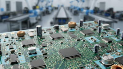
Overview of Standard PCB Fabrication Processes and Their Applications
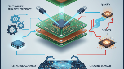
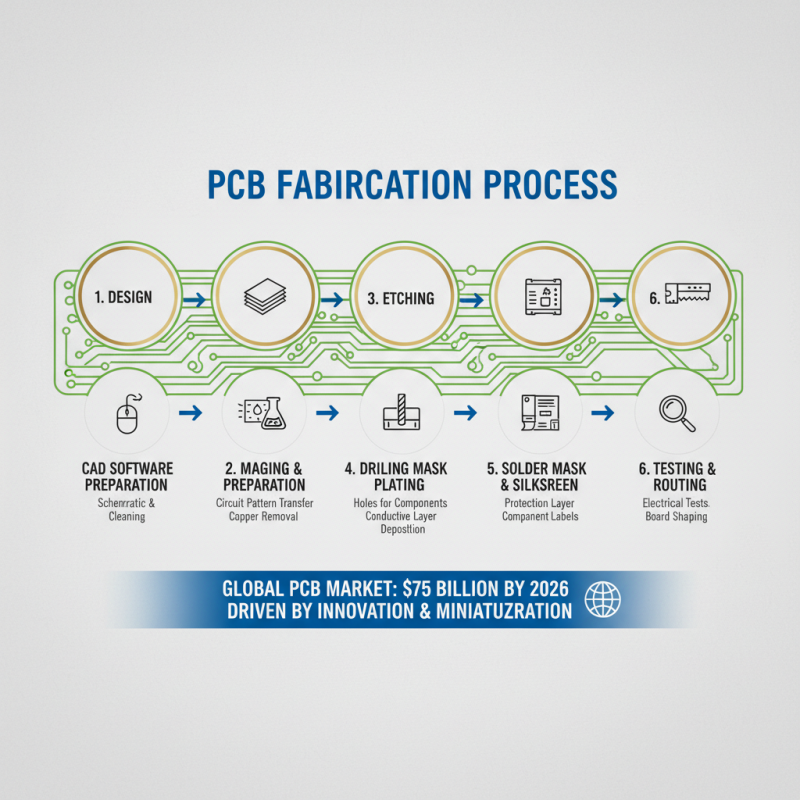
PCB fabrication is a crucial process in the electronics industry, impacting the performance of various devices. According to a report from ResearchAndMarkets, the global PCB market is expected to reach $75 billion by 2026, driven by innovations and demand for miniaturization. Understanding standard PCB fabrication processes helps businesses adapt to market needs.
Key processes include etching, drilling, and plating. Etching removes unwanted copper from the copper-clad laminate, creating the circuit design. Drilling is necessary for component placement and interconnections. Plating adds a layer of metal to enhance conductivity. Interestingly, a survey by IPC found that about 30% of engineers face challenges in achieving optimal design due to fabrication limitations. These hurdles often require rethinking designs, which can lead to delays and increased costs.
Applications for PCBs range from consumer electronics to medical devices. For instance, multi-layer PCBs are essential in smartphones, accommodating dense circuitry in limited space. Yet, the complexity of these processes can create setbacks. A gap exists between design capabilities and fabrication realities, prompting a need for improved collaboration between designers and manufacturers. Addressing these challenges can enhance product reliability and performance.
Advanced Techniques: HDI, Multilayer, and Flexible PCBs Explained
High-Density Interconnect (HDI) technology is gaining traction in PCB fabrication. This technique uses smaller traces and pads, allowing more components to fit into a smaller area. Designers can create compact and powerful devices. However, the manufacturing process can be more complex and costly. Balancing performance and cost is essential.
Multilayer PCBs are another advanced technique. These boards consist of multiple layers of conductive and insulating material, allowing complex circuits. They enable the use of more intricate designs and functionalities. However, achieving the right layer alignment and ensuring reliability can be challenging. Mistakes in layering can lead to significant issues.
Flexible PCBs provide unique advantages. They can bend and twist, making them suitable for compact spaces. These boards are increasingly used in wearables and portable devices. Despite their benefits, they often pose difficulties in handling and manufacturing. Ensuring durability while maintaining flexibility requires careful consideration.
Emerging Technologies in PCB Fabrication: 3D Printing and Automation
The landscape of PCB fabrication is evolving rapidly. One of the most exciting advancements is 3D printing. This technology allows for intricate designs that traditional methods struggle to achieve. Imagine creating a multi-layer PCB in one single print. It reduces waste and time significantly. However, the quality can vary. There are still questions about durability and reliability.
Automation is another trend reshaping production. Machines can now handle repetitive tasks with precision. This increases efficiency and reduces human error. Yet, it raises concerns about the workforce. As robots take over, jobs may disappear. Companies must find a balance between innovation and employment.
These technologies promise significant improvements. But with advancements come challenges and uncertainties. As the industry embraces these changes, reflection is crucial. Are we ready for this shift? Time will tell if these techniques meet the needs of future innovations.
Cost-Effectiveness Analysis of Various PCB Manufacturing Methods
Cost-effectiveness in PCB manufacturing is crucial for various industries. Each fabrication method has its unique strengths and weaknesses. For example, traditional subtractive methods can be expensive. They often lead to material wastage. Data shows that this can increase costs by up to 30% in mass production.
On the other hand, additive manufacturing techniques are gaining traction. They offer reduced material waste and can be more adaptable. According to recent studies, companies using these methods saw a 20% reduction in production costs. However, the initial investment for this technology can pose challenges. Innovation is costly, and not all companies can afford it.
Moreover, evaluating processes such as screen printing or laser direct imaging reveals varying impacts on overall cost. Screen printing, while inexpensive, may not deliver high precision. Many firms have reported quality issues that lead to reworks. This can offset savings from lower initial costs. Such inconsistencies remind us to look closely at long-term implications when choosing a PCB fabrication method.