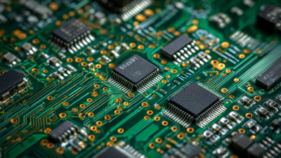
Top Tips for Successful PCB Board Design and Common Mistakes to Avoid
In the rapidly evolving field of electronics, successful PCB board design is pivotal to ensuring the functionality and reliability of myriad devices, from consumer gadgets to industrial machinery. As the demands for smaller, more efficient, and high-performance electronic systems increase, so does the complexity of PCB design. According to a recent report by IPC, the global PCB market is expected to reach $85 billion by 2027, highlighting the critical need for optimized design practices that can keep pace with this growth.
Expert insight from Dr. Emily Tran, a recognized authority in PCB design, underscores the importance of meticulous planning and execution. She states, “Effective PCB board design is not just about layout; it encompasses a comprehensive approach that considers thermal management, signal integrity, and manufacturability from the outset.” This perspective emphasizes that understanding the common pitfalls in the design process can greatly enhance the efficiency and performance of electronic products.
As we delve into the top tips for successful PCB board design and the common mistakes to avoid, it is vital for designers to adopt a strategic mindset, leveraging best practices and expert recommendations to create boards that meet today's stringent standards and customer expectations. By doing so, engineers can turn potential challenges into opportunities for innovation and excellence in the ever-competitive landscape of electronics.

Essential Principles of PCB Board Design for Success
When it comes to successful PCB board design, adhering to essential principles is crucial. First and foremost, understanding the electrical requirements of your project is vital. This includes accurately calculating power and signal integrity to ensure that the board functions correctly under various conditions. Designers should aim to create a clear schematic before diving into layout tasks, allowing for better visualization of component placement and interconnections. This approach not only streamlines the design process but also minimizes the chances of design faults that could lead to costly revisions.
Another key principle is the effective management of space. Keeping the layout organized and avoiding overcrowding is essential for both functionality and manufacturability. Properly routing traces to minimize interference and ensuring adequate space around high-frequency components can significantly enhance performance. Additionally, taking thermal management into account can prevent overheating and prolong the life of the PCB. By maintaining these principles, designers can achieve a balanced, high-performing board that meets industry standards and project specifications, ultimately setting the stage for success in their electronic designs.
Common Mistakes in PCB Design and How to Avoid Them
When it comes to PCB design, avoiding common missteps can significantly enhance the success of a project. One such mistake is neglecting thorough component placement planning. According to a recent industry report by IPC, approximately 35% of design issues stem from improperly placed components, which can lead to signal integrity problems and increased electromagnetic interference (EMI).
To mitigate this risk, designers should prioritize the layout stage, ensuring that critical components are strategically placed to minimize trace lengths and optimize circuit performance.
Another prevalent error in PCB design is failing to account for thermal management. Overheating can compromise the functionality and lifespan of a board, yet a survey by the IEEE found that nearly 40% of engineers overlook thermal considerations during the design phase. Effective thermal management begins with understanding the heat generation of each component and implementing adequate spacing, thermal vias, and heat sinks as necessary. Incorporating simulation tools to evaluate thermal performance early in the design process enables engineers to proactively address potential overheating issues.
Additionally, underestimating the importance of design rule checks can lead to significant delays and added costs. A study published by the Design Automation Conference reveals that nearly 30% of PCB redesigns result from overlooked design rules, which can include trace widths, hole sizes, and layer stackup configurations. By integrating automated design rule checks throughout the design cycle, engineers can catch these issues before reaching the fabrication stage, ensuring a smoother development process and reducing the likelihood of costly mistakes.
Best Practices for Layout and Schematic Design in PCBs
When it comes to PCB layout and schematic design, adhering to best practices can significantly impact the performance and reliability of your circuit boards. One essential principle is to keep the layout as compact as possible while ensuring that components are strategically placed to minimize signal interference. Maintaining short trace lengths can reduce inductance and capacitance effects, which is crucial for high-speed signals. Ensure that the return paths are well-defined to prevent ground bounce and other noise-related issues. Additionally, employing a consistent grid system helps in aligning components uniformly, improving both aesthetics and functionality.
Another critical aspect is the organization of the schematic. A well-structured schematic not only aids in troubleshooting but also enhances the communication of your design intent to others. Use clear labeling for all components and signals, and group related components together to create logical sections. It’s also important to implement sufficient spacing to avoid confusion between traces, especially when dealing with complex designs. By addressing these layout and schematic practices, you can avoid common pitfalls such as design errors or difficulties in manufacturing, ultimately leading to a more successful PCB project.
Top Tips for Successful PCB Board Design and Common Mistakes to Avoid - Best Practices for Layout and Schematic Design in PCBs
| Design Aspects |
Best Practices |
Common Mistakes |
| Schematic Design |
Use clear labeling and maintain a consistent layout |
Neglecting to add comments for complex sections |
| Component Placement |
Place components logically and group similar signals |
Random placement without considering signal integrity |
| Routing |
Use wide traces for power and ground; minimize vias |
Overlooking the importance of trace width and length |
| Ground Planes |
Incorporate solid ground planes to reduce EMI |
Isolating analog and digital grounds improperly |
| Design Rule Check (DRC) |
Run DRC frequently during design phases |
Ignoring DRC warnings until the end of the design |
Importance of DFM and DFT in PCB Design Process
In the realm of PCB design, the integration of Design for Manufacturing (DFM) and Design for Testability (DFT) is crucial for enhancing product efficiency and reducing costs. DFM focuses on the manufacturability of the PCB, ensuring that the design can be produced reliably and economically. According to a report by IPC, nearly 60% of PCB design issues arise from manufacturability problems, leading to increased production times and costs. By prioritizing DFM, designers can streamline the manufacturing process, minimize waste, and significantly improve yield rates.
On the other hand, DFT is essential for ensuring that the final product can be easily tested for functionality and reliability. A study from IEEE indicates that products incorporating DFT principles can reduce testing time by up to 30%, allowing for faster time-to-market. This approach not only aids in identifying defects early in the manufacturing process but also facilitates better maintenance and upgrades of the PCB over its lifecycle. By adopting both DFM and DFT strategies, designers can create more robust, reliable, and cost-effective PCB solutions, leading to greater customer satisfaction and reduced production costs.
Techniques for Effective Testing and Validation of PCB Designs
Effective testing and validation of printed circuit board (PCB) designs are crucial steps in the development process. One of the most important techniques is simulation. Utilizing advanced simulation software allows designers to create virtual models of their PCBs, enabling them to analyze electrical performance, thermal characteristics, and mechanical stability before manufacturing. This proactive approach helps identify potential issues early, thereby reducing the amount of costly iteration during physical prototyping.
In addition to simulation, conducting thorough prototype testing is vital. After creating a physical prototype, engineers should perform a series of tests under various conditions to gauge its performance. This includes checking for signal integrity, power distribution, and thermal management. Employing methodologies like design for testability (DFT) can enhance the testing process by ensuring that critical areas of the PCB are easily accessible for measurement and validation. Overall, a combination of simulation and rigorous testing will ensure that the PCB design is solid, functional, and ready for production.