Why Printed Circuit Boards Are Essential for Modern Electronics Innovation
In the rapidly evolving landscape of modern electronics, the significance of the
printed circuit board (PCB) has never been more pronounced.
As technology advances, the demand for efficient, reliable, and compact electronic designs
continues to grow, making PCBs an essential component in driving innovation.
Dr. Emily Chen, a renowned expert in the field of electronic engineering,
once stated, “Without printed circuit boards, the intricate functionalities and seamless
operation of today’s gadgets would simply be impossible.” Her insight underscores the pivotal
role that PCBs play in not only connecting electronic components but also in enabling the
development of cutting-edge technology.
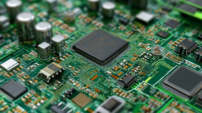
PCBs serve as the backbone of virtually all electronic devices, from smartphones to
artificial intelligence systems. They facilitate the miniaturization of circuits while
enhancing performance and reducing manufacturing costs, thereby paving the way for advanced
innovations. As we delve deeper into the intricacies of PCBs, it becomes clear that they
are not merely a practical solution, but a driving force behind the technological advancements
that shape our modern world. Their versatility and adaptability ensure
that as we explore new frontiers in electronics, printed circuit boards will remain at the forefront,
continually inspiring creativity and transforming ideas into reality.
The Role of Printed Circuit Boards in Integrating Complex Electronics
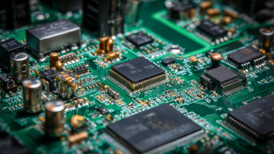
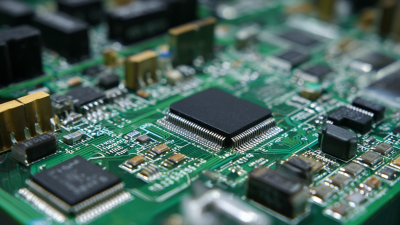
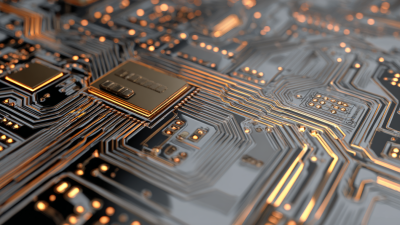
Printed Circuit Boards (PCBs) serve as the backbone of modern electronics, facilitating the integration of complex components into a cohesive system. By providing a structured platform for mounting and connecting electronic components, PCBs enable intricate circuitry to be compactly arranged, thus reducing size and improving performance. The precision of printed circuit boards allows for the effective routing of electrical signals, ensuring that devices function seamlessly without interference, which is crucial in high-frequency applications.
Moreover, the versatility of PCBs supports advancements in technology across various industries, from consumer electronics to medical devices. With the growing demand for smaller, more efficient devices, PCBs can be designed with innovative substrates and materials that enhance thermal management and electrical performance. This adaptability not only fosters innovation but also allows engineers to push the boundaries of what is possible, leading to the development of sophisticated systems such as smartphones and IoT devices that require reliable and compact circuit designs. Ultimately, the role of printed circuit boards in integrating complex electronics is foundational to the progress of electronics innovation.
Why Printed Circuit Boards Are Essential for Modern Electronics Innovation
| Dimension |
Description |
Importance |
| Layer Count |
Number of layers in PCB construction |
Determines circuit complexity and density |
| Material Type |
Type of material used (e.g., FR-4, Rogers) |
Affects thermal conductivity and electrical performance |
| Trace Width |
Width of the electrical traces on the PCB |
Impacts current carrying capacity and resistance |
| Via Type |
Types of vias used (e.g., through-hole, blind, buried) |
Essential for interconnecting layers effectively |
| Surface Finish |
Surface treatment applied to the PCB pads |
Affects solderability and corrosion resistance |
| Impedance Control |
Management of the circuit's impedance |
Ensures signal integrity for high-speed applications |
| Thermal Management |
Methods used to dissipate heat |
Crucial for preventing overheating and device failure |
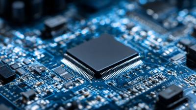
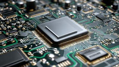
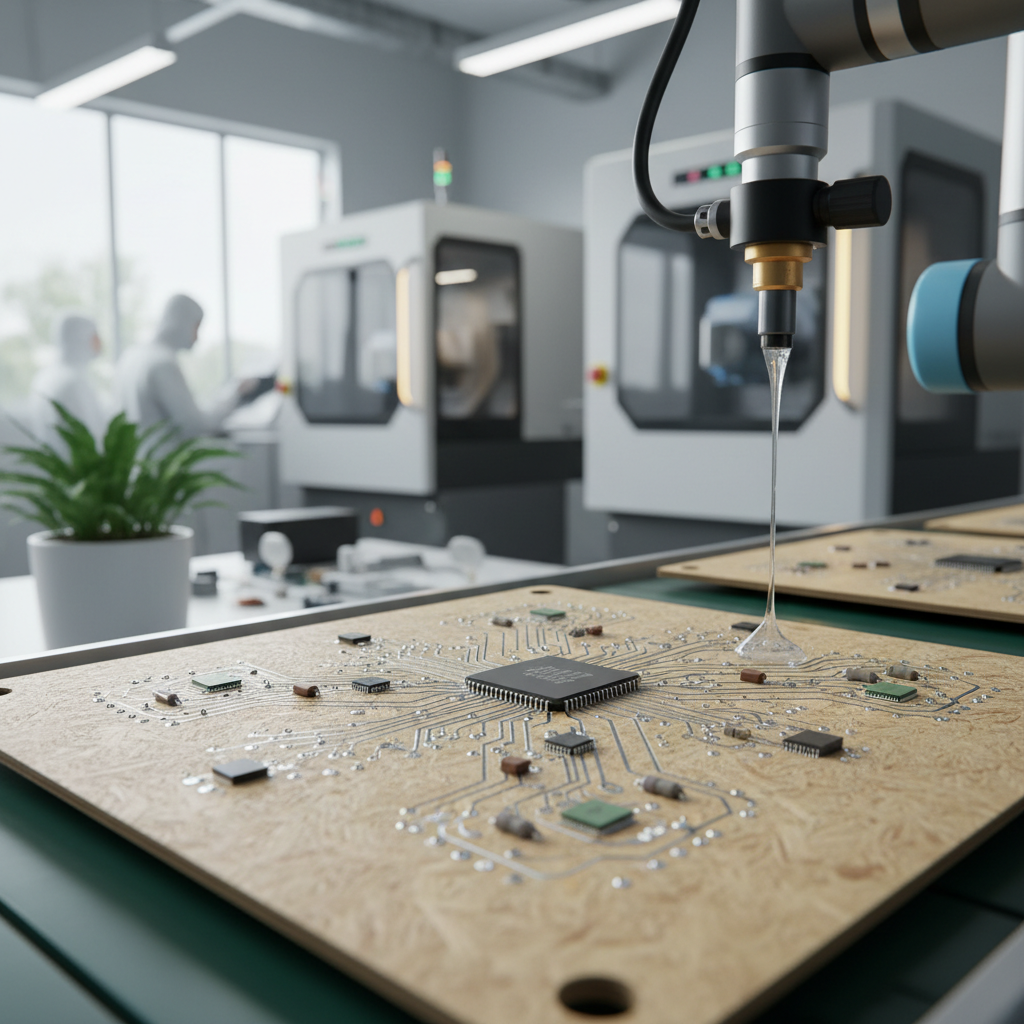
Advancements in PCB Technology Driving Electronic Miniaturization
The miniaturization of printed circuit boards (PCBs) is at the forefront of driving efficiency and reliability across various industries. As electronic devices become smaller and more complex, advancements in PCB technology enable manufacturers to create compact solutions without compromising performance. Techniques such as substrate-like PCBs are revolutionizing production methods, facilitating the development of high-density interconnections that allow for increased functionality within reduced dimensions.
The market for substratelike PCBs is projected to experience substantial growth, with expectations to reach approximately USD 8.9 billion by 2034, reflecting a remarkable compound annual growth rate (CAGR) of 19.5%. This growth is indicative of the broader trend in electronics, where miniaturization is not just a preference but a necessity for achieving better product integration and user experience. Innovations in technologies like SAP and mSAP have transformed the manufacturing landscape, offering enhanced capabilities that propel the electronics industry toward a future of increased efficiency, reliability, and unprecedented levels of integration.
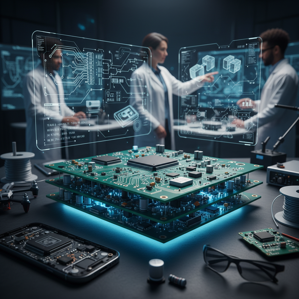
Impact of PCBs on Versatility in Modern Consumer Devices
Printed Circuit Boards (PCBs) play a pivotal role in the versatility of modern consumer devices, driving innovation across various electronics sectors. The increasing complexity and functionality of devices have made the demand for advanced PCB technologies greater than ever. As manufacturers strive to create slimmer, more efficient products, the ability of PCBs to accommodate multiple electronic components in a compact space becomes crucial. This versatility not only enhances product design but also allows for improved performance and longer battery life, which are essential attributes for today's consumers.
Recent industry reports highlight the competitive landscape among PCB manufacturers. Companies are focusing on optimizing production processes and expanding their capabilities to meet evolving market demands. As innovations in PCB technology continue to emerge, including the use of advanced materials and multi-layered designs, these firms are setting the stage for groundbreaking developments in consumer electronics. The emphasis on flexibility and adaptability in PCB design ensures that manufacturers can keep pace with the rapid advancements in technology, ultimately leading to a more dynamic and exciting electronic ecosystem.
Sustainability Considerations in PCB Manufacturing and Design
The shift toward sustainability in the manufacturing and design of printed circuit boards (PCBs) is becoming increasingly important in the realm of modern electronics. As industries recognize the environmental impact of electronic waste and hazardous materials, efforts are being made to implement eco-friendly practices. This includes utilizing biodegradable substrates, reducing the use of toxic chemicals, and optimizing designs to minimize material waste. By adopting such practices, manufacturers can decrease the carbon footprint associated with PCB production, paving the way for a more sustainable future.
Innovative design strategies also play a crucial role in fostering sustainability in PCB technology. For instance, integrating modular designs allows for easier repairs and upgrades, thereby extending the lifespan of electronic devices and reducing the volume of discarded products. Additionally, investing in recycling technologies enables the recovery of precious metals and materials from end-of-life PCBs, effectively promoting a circular economy. As electronic devices continue to evolve, embracing sustainability in PCB manufacturing and design will not only support environmental responsibility but also drive innovation within the electronics industry.
Future Trends: The Evolution of PCBs in Next-Gen Electronics
The evolution of printed circuit boards (PCBs) is crucial for the advancement of next-generation electronics, particularly in the automotive sector. The global automotive PCB market is projected to grow from USD 10.98 billion in 2025 to USD 18.14 billion by 2034, reflecting the increasing demand for sophisticated electronic systems in vehicles. This growth is fueled by innovations such as next-gen LiDAR technology, which enhances autonomous systems with improved range and resolution, necessitating more advanced PCB designs that integrate seamlessly with these technologies.
Moreover, the shift towards AI-driven solutions in industries, highlighted by events like COMPUTEX 2025, is steering the development of PCBs towards greater programmability and connectivity. As the automotive industry adapts to evolving consumer preferences, especially with the emergence of electric and autonomous vehicles, the need for next-gen electrical/electronic architectures is paramount.
Tips: When designing PCBs for next-gen applications, consider the importance of advanced semiconductor packaging that transitions from basic 1D designs to innovative 3D hybrid bonding. This approach not only enhances performance but also supports the intricate requirements of modern electronics. Additionally, keep an eye on the integration of remote monitoring technologies in wearables, as these will play a significant role in the future electronic landscape. Adapting your PCB designs to these trends will ensure your products remain competitive and viable in a rapidly changing market.