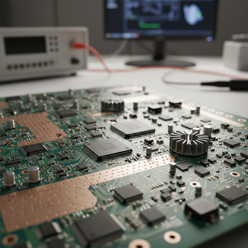
What is PCB Layout and How Does it Impact Circuit Design?
PCB layout is critical in the field of circuit design. It refers to the arrangement of electronic components on a printed circuit board. A well-designed PCB layout can enhance performance and reliability. Poor layouts can lead to issues like signal interference or overheating.
Designing a PCB layout involves understanding component placement, routing, and ground planes. Engineers must consider electromagnetic compatibility and thermal management. They face challenges in balancing space and functionality. Designing a layout that accommodates all parts is not always straightforward.
Mistakes in PCB layout can be costly. They may lead to circuit failure or production delays. Engineers often learn from these setbacks. Continuous improvement in layout strategies is crucial. Reflecting on past designs can lead to better outcomes in future projects. Therefore, PCB layout significantly impacts overall circuit design success.
Understanding PCB Layout: Definition and Importance in Electronics
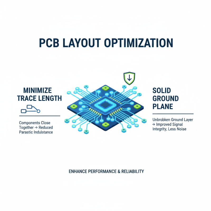
Understanding PCB layout is crucial in electronics. It refers to the arrangement of electronic components on a printed circuit board. A well-structured layout can enhance the performance of the circuit significantly. According to a report by IPC, poorly designed PCB layouts can lead to a 30% increase in manufacturing costs. This highlights the importance of thoughtful design practices.
Moreover, the layout affects signal integrity and electromagnetic interference (EMI). A study by Altium reveals that nearly 50% of design failures stem from layout issues. Components placed too close can cause noise. The right spacing and routing can minimize this risk. Incorporating ground planes and proper trace widths can improve performance.
Many engineers struggle with layout challenges. It often requires a balance between functionality and manufacturability. Mistakes in routing or component placement can lead to big problems. Time spent on layout can save time in production. Reflecting on your design process can uncover flaws. Engaging in peer reviews may catch overlooked details. Ultimately, a thoughtful PCB layout is vital for success in modern electronics.
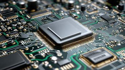
Key Elements of PCB Layout: Components, Traces, and Design Rules
PCB layout is a critical part of circuit design. It involves arranging components and wiring them efficiently. Effective layout ensures that signals pass through the correct paths. Poor layout can lead to noise and interference. It may also cause overheating and short circuits.
Key elements in a PCB layout include components, traces, and design rules. Components should be placed based on their function. For example, keep capacitors close to power pins. This helps to minimize noise. Traces connect these components. They should be as short and direct as possible. Wider traces can handle more current, so consider the current requirements.
**Tip:** Always check design rules before finalizing your layout. This can prevent costly errors. Use design software that highlights rule violations. It can save time and effort. Remember, not every design is perfect on the first try. Review and revise as needed. Small changes can make a big difference.
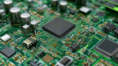
Impact of PCB Layout on Circuit Design
The Role of PCB Layout in Circuit Performance and Stability
The layout of a printed circuit board (PCB)
plays a crucial role in determining the performance of electronic circuits. A well-designed layout can enhance signal integrity and reduce noise. Poor routing decisions, however, may lead to cross-talk or interference. The placement of components affects how signals travel. If parts are too far apart, this could cause delays in performance.
Another concern is the thermal management of a PCB. Proper layout ensures that heat dissipation is effective. Components that generate heat need to be spaced appropriately. Overheating can lead to failure, affecting overall stability. Designers sometimes overlook these factors, leading to performance issues during testing.
Reflections on past projects reveal common mistakes. Many designers fail to consider the ground plane layout or trace widths. These oversights can dramatically impact circuit stability. Additionally, the use of vias needs careful planning. A poorly placed via can introduce resistance and affect signal quality. Continuous learning and iteration are necessary for improvement in PCB design.
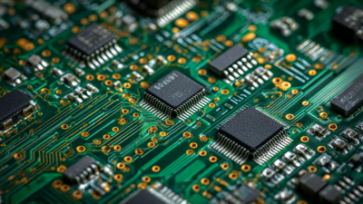
Tools and Software for Effective PCB Layout in Circuit Design
When designing printed circuit boards (PCBs), the right tools and software significantly enhance the layout process. Effective PCB layout tools streamline design, allowing engineers to create intricate circuits efficiently. Features like auto-router and design rule checks are essential. They help in avoiding common mistakes, but not all tools are user-friendly. Some platforms can feel overwhelming due to their complexity.
Simulation software plays a crucial role in the design phase. It allows engineers to test circuits before physical production. However, simulation inaccuracies can lead to flawed designs. Often, it’s easy to overlook minor details that result in costly errors. A balance between innovation and practicality is necessary in tool selection.
Collaboration is another key factor. Many PCB design tools offer cloud-based features for team projects. This can facilitate communication but may also present challenges in version control. Without proper management, confusion can arise among team members. A collective reflection on these issues can lead to improved workflows and ultimately ensure a successful circuit design.