What is PCB Fabrication and How Does it Impact Electronics?
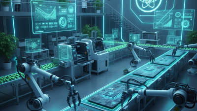
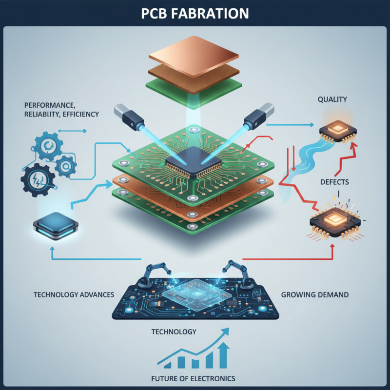
PCB fabrication is a critical process in the electronics industry. It involves creating printed circuit boards that serve as the backbone of modern devices. This fabrication process directly impacts the performance, reliability, and efficiency of electronic products.
During PCB fabrication, various materials are layered and etched to produce intricate designs. This complexity allows devices to become smaller and more powerful. However, the quality of fabrication can vary. Inconsistent processes can lead to defects, affecting device functionality. Understanding these risks is essential for manufacturers.
As technology advances, PCB fabrication continues to evolve. New techniques are emerging, aiming for greater precision and lower costs. The growing demand for electronics pushes innovation further. Companies must reflect on their fabrication methods to stay competitive. It's vital to balance speed with quality. The future of electronics relies heavily on improving PCB fabrication processes.
What is PCB Fabrication: Definition and Overview
PCB fabrication refers to the process of manufacturing printed circuit boards. These boards are critical in the electronics industry. They connect various components, allowing devices to function. The PCB market is expected to grow from $60 billion in 2023 to $100 billion by 2030, highlighting its significance.
During PCB fabrication, layers of materials are assembled. Common materials include copper and resin. The quality of these materials influences the performance of electronic devices. Poor quality can lead to failures or inefficiencies. An industry report indicated that 40% of electronics failures originate from PCB issues. This statistic underscores the necessity for stringent quality control.
Moreover, the complexity of PCB designs has increased. Many modern devices require multi-layered boards. Each additional layer complicates the fabrication process, increasing production time. Some manufacturers may take shortcuts in these intricate designs, risking quality. Consequently, ensuring efficient fabrication practices is crucial for longevity and reliability in electronics.
Key Materials Used in PCB Manufacturing and Their Properties
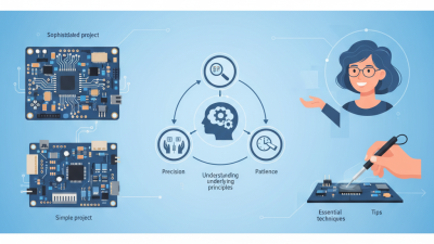
Key materials used in PCB manufacturing are crucial for the performance and reliability of electronic devices. The most common substrate material is FR-4, a glass-reinforced epoxy laminate. It provides excellent insulation and mechanical strength. However, FR-4 can sometimes lose structural integrity at high temperatures, which can be a concern in demanding applications.
Another key material is copper. It serves as the conductor that carries electrical signals. The thickness of the copper layer significantly affects the overall performance of the PCB. Thinner layers may not handle high currents well, leading to potential failures. Understanding the requirements of your project is vital when selecting copper thickness.
Tips:
Always review material specifications before choosing them for your PCB. Check for compatibility with your application. Additionally, consult with experienced manufacturers; they can offer insights into material behavior under various conditions, helping mitigate potential issues. Keep in mind that even small changes in materials can result in significant impacts on functionality.
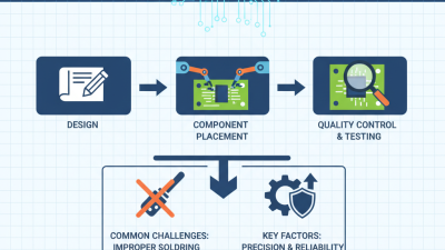
The PCB Fabrication Process: Step-by-Step Breakdown
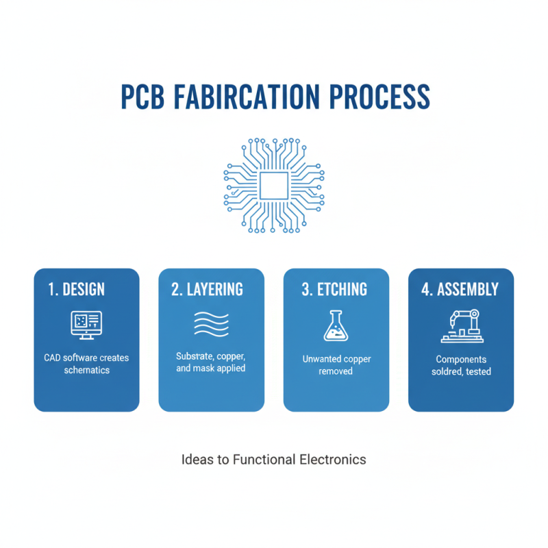
The PCB fabrication process is crucial for electronics. It transforms ideas into functional circuit boards, enabling electronic devices to operate. The steps involve design, layering, etching, and assembly, each vital for a successful PCB.
Designing begins with a schematic layout. Software tools help create precision placements for components. According to industry reports, about 70% of errors occur during this phase. Double-checking is key. A misplaced component can derail the whole project.
Layering follows, where substrates like FR-4 are used. They provide electrical insulation and strength. An expert noted that over 40% of production time goes into preparing these layers. Insufficient attention here can lead to costly mistakes.
Etching removes excess copper. This step shapes the circuits. It's vital but can be wasteful if not managed carefully. Manufacturers often see over 10% material loss, suggesting a need for better planning to minimize waste.
**Tips:** Always validate design files before moving to fabrication. Collaborating closely with manufacturers can help identify potential issues early. Keep revising your processes to lessen material loss during production.
Impact of PCB Design on Electronics Performance and Reliability
PCB design plays a crucial role in determining the performance and reliability of electronic devices. A well-thought-out design ensures signals can travel efficiently. Good layout minimizes interference, which is essential for high-speed applications. Poor design, on the other hand, can lead to delays and failures. For instance, improper trace widths may cause overheating. This can be detrimental to sensitive components.
Thermal management is another critical element. A PCB's heat dissipation capabilities affect overall functionality. If the design lacks adequate cooling features, devices may suffer from performance losses. In high-demand scenarios, like gaming, this issue becomes more prominent. Engineers need to be careful with component placement and spacing.
There are also challenges related to manufacturing tolerances. Inconsistent dimensions can result in assembly issues. This may lead to short circuits or unreliable connections. Designers must consider these factors during the initial design stage. Simulations can provide insights but may not catch every potential issue. Regular review and testing are vital for ensuring the design holds up in real-world applications.
What is PCB Fabrication and How Does it Impact Electronics? - Impact of PCB Design on Electronics Performance and Reliability
| Dimension |
Description |
Impact on Electronics |
| Layer Count |
Number of layers in a PCB |
Higher layers can reduce signal interference and improve circuit density. |
| Material Type |
Type of material used (e.g., FR-4, Rogers) |
Affects thermal performance and reliability of connections. |
| Trace Width |
Width of the copper traces |
Impacts current-carrying capacity and heat generation. |
| Via Type |
Types of vias (e.g., through-hole, blind, buried) |
Affects signal integrity and space efficiency. |
| Finish Type |
Surface finish (e.g., HASL, ENIG) |
Affects solderability and corrosion resistance. |
| Design Complexity |
Level of detail in design (e.g., components, layout) |
Higher complexity can improve functionality but complicates manufacturing. |
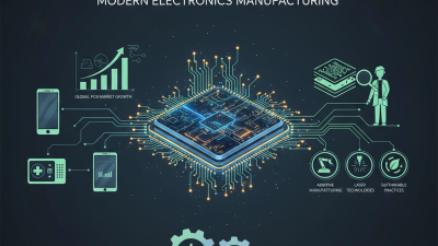
Market Trends: Growth and Innovations in PCB Fabrication Industry
The PCB fabrication industry is experiencing rapid growth, driven by increased demand for electronics. Innovations in materials and processes are emerging at a fast pace. For example, advanced materials like flexible substrates are changing the game. They allow for more complex designs and lightweight products. This shift is evident in industries like automotive and consumer electronics. Manufacturers are adapting to keep up with trends.
Another noteworthy trend is automation in PCB manufacturing. Automation enhances speed and efficiency while reducing human error. However, there are challenges. Not all manufacturers have the resources for such investments. Smaller companies may struggle to compete. This gap in capabilities can impact their market position. Embracing innovation is crucial yet not universally achievable.
Sustainability is also becoming a focal point in PCB fabrication. Eco-friendly materials and processes are gaining traction. Manufacturers are looking to reduce waste and energy consumption. Still, the transition can be rocky. Some processes still rely heavily on traditional methods. Balancing innovation with sustainable practices remains a challenge for the industry. This ongoing evolution reflects the dynamic nature of PCB fabrication.