What Is PCB Design Software and How Does It Work?
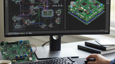
Modern electronic products begin with a quiet, detailed task: arranging copper traces, components, and connection points on a digital board. This is where pcb design software becomes essential. It helps engineers convert circuit diagrams into manufacturable printed circuit boards. The process includes schematic capture, component placement, routing, design-rule checking, simulation, and production-file generation. A laptop motherboard may contain thousands of connections. One misplaced trace can create heat, noise, or complete failure.
Industry data shows why this work matters. The World Semiconductor Trade Statistics (WSTS) Spring 2025 Forecast projected global semiconductor sales of approximately $697 billion in 2025. More powerful chips increase demands on board layout, signal integrity, thermal control, and power delivery. PCB design software responds by automating repetitive checks and displaying problems before fabrication. IPC’s 2024 Global Sentiment of the Electronics Industry report also reflects continuing pressure around costs, supply chains, and production efficiency. Better design decisions can reduce expensive prototype revisions.
Still, software is not a substitute for engineering judgment. It cannot fully understand every material choice, assembly constraint, or real-world failure. That part remains human. Engineers must verify footprints, review manufacturing tolerances, and test the completed board. A clean screen does not guarantee a reliable product. In this guide, we will examine how pcb design software works, which core features matter, and how professional teams use it from concept to production. The answer is practical, not magical. Mistakes still happen. The goal is to catch them earlier.
Definition and Purpose of PCB Design Software
What Is PCB Design Software and How Does It Work?
Definition and Purpose of PCB Design Software
PCB design software is a digital workspace for creating printed circuit boards. It connects electrical planning with physical construction. Designers draw a schematic to show how components should communicate. The software then turns that plan into a board layout. Copper tracks, pads, vias, layers, and mounting holes receive precise positions.
Its main purpose is to reduce design errors before manufacturing begins. Rule-checking tools can identify unwanted connections, narrow clearances, missing power paths, and incorrectly placed components. Layer views also reveal whether a signal crosses the board safely. For example, a designer may inspect a high-speed trace near a noisy power section. Small details matter. A crowded corner can affect assembly and long-term reliability.
Tips: Set board rules before routing. Check clearance values against the manufacturer’s requirements. Review heat-producing components and connector locations early. Keep a clear naming system for nets and footprints. It saves time later.
The workflow is useful, but not flawless. A green rule-check report does not guarantee a dependable product. It may miss heat buildup, mechanical strain, or a footprint that feels awkward during assembly. Designers should inspect the board visually and compare it with the enclosure, datasheets, and production limits. A second review often finds what software overlooks. That human pause is easy to skip. It should not be.
PCB Design Software: Simulated RC Low-Pass Response
PCB design software can simulate circuit behavior before a board is manufactured. This waveform shows the calculated output of a 1 kΩ resistor and 100 nF capacitor connected to a 3.3 V step input. The output rises exponentially, reaching approximately 63.2% of its final value after one time constant, τ = RC = 0.1 ms.
Core Tools and Features in PCB Design Programs
PCB design software converts an electrical idea into a manufacturable circuit board. Its core workflow begins with schematic capture, where engineers place symbols and connect nets. Component libraries store footprints, ratings, and land patterns. A small mismatch here can create an expensive production error.
Layout tools then arrange components and route copper traces across multiple layers. Designers control clearance, trace width, via size, impedance, and thermal paths. Design-rule checking automatically flags short circuits, missing connections, and spacing violations. Simulation tools can examine voltage drops, timing, heat, and signal integrity before fabrication. That matters. Manual review still matters.
Collaboration features are becoming equally important. Version control records design changes, while constraint managers preserve manufacturing rules across teams. Export tools generate Gerber or ODB++ files, drill data, and bills of materials for production. A 2024 Global EDA Market estimate placed the sector at roughly 13 billion dollars in 2023, reflecting growing demand for digital verification. IPC’s 2024 electronics industry survey also highlighted persistent material constraints and skilled-labor shortages. These pressures make automation useful, but not perfect. In practice, I would never trust an unchecked autorouter or library entry. A clean visual layout can still hide weak grounding, poor heat dissipation, or an incorrect footprint. Experienced engineers inspect critical nets manually and compare fabrication outputs with the original schematic.
The Step-by-Step PCB Design Process
PCB design software turns circuit ideas into manufacturable board layouts. The process begins with a schematic, where engineers define components and electrical connections. Each symbol must match a correct physical footprint. A small mismatch can delay assembly.
Designers then set board dimensions, layer count, spacing rules, and material requirements. They place connectors first, because their positions affect the enclosure. Sensitive circuits need short paths and careful separation from noisy power sections. Routing follows, using copper traces, vias, and defined ground paths. Power traces usually need more width than signal traces. The software checks clearance, unconnected nets, and other manufacturing risks through design rule checks. These checks help, but they are not perfect. Human review still matters. A clean screen does not guarantee a reliable board.
Tips:
Name nets clearly. Keep related parts close. Use realistic trace widths. Check heat paths early. Print the layout at full scale and inspect connector access. This simple test often exposes awkward placement. Before fabrication, designers review the layer stack, drill data, solder mask openings, and assembly drawings. They may run signal or thermal simulations when performance demands it. A prototype then reveals practical issues, such as unexpected noise or difficult soldering. Engineers revise the layout based on measured results, not assumptions. That feedback loop is where PCB design becomes dependable.
How PCB Software Converts Schematics into Board Layouts
PCB design software turns an electrical schematic into a physical board layout. It does not simply draw connected lines. The software reads symbols, footprints, net names, and component values. It then builds a connectivity model for the proposed circuit. This model becomes the foundation for component placement and routing.
A designer usually begins by assigning each component a verified footprint. A resistor may need two pads, while a processor can require hundreds. The software checks whether every schematic pin matches its physical pad. Errors often appear here. A missing pin, wrong package, or reversed connector can damage an otherwise careful design.
Placement follows electrical and mechanical requirements. High-speed parts stay close to supporting capacitors. Power paths need wide copper traces. Sensitive signals may require controlled spacing and separate routing areas. The tool then records connections as traces, vias, copper zones, and board outlines. Design-rule checks inspect clearance, unconnected nets, hole sizes, and manufacturing limits. I have found these checks valuable, but they cannot replace engineering judgment. A layout can pass every rule and still suffer from heat, noise, or poor assembly access. Engineers should review the board in three dimensions and compare it with the real enclosure. Rechecking the schematic after layout is worthwhile. Small assumptions can survive longer than expected.
File Formats, Design Rules, and Manufacturing Outputs
What Is PCB Design Software and How Does It Work?
PCB design software turns an electrical concept into a manufacturable board layout. It connects schematics, copper traces, component footprints, and production files. A reliable workflow begins with suitable file formats. Native project files preserve editing history and design settings. Gerber files describe copper, solder mask, silkscreen, and board outlines. Drill files define hole locations and sizes. Some manufacturers accept structured formats for richer design data.
Never assume an export worked.
Open every output in an independent viewer. Check layer names, units, board dimensions, and missing apertures. I have found small outline errors during this step, even after a clean software check. That experience makes visual inspection essential, not optional.
Tips: Keep a written export checklist. Include board thickness, copper weight, tolerances, and finish requirements. Design rules control clearance, trace width, hole size, and spacing near the board edge. They reduce manufacturing risks, but they are not universal. A rule that passes in one factory may fail in another. Ask the manufacturer for current capability data before routing dense areas. Then review the final plots and drill map together. The process feels repetitive. It still prevents expensive revisions.