What is PCB Assembly and How Does It Work?
In the world of electronics, PCB assembly is crucial for creating functional devices. Dr. Emily Chen, an expert in circuit design, once stated, “PCB assembly is the heart of any electronic product.” Her insights highlight the importance of this process.
PCB assembly involves several steps, including soldering components onto printed circuit boards. Each step requires precision and attention to detail. Issues can arise during assembly, leading to defects that may affect product performance. This complexity makes the assembly process both challenging and fascinating.
Understanding both the technology and common pitfalls in PCB assembly is essential. Ignoring small details can lead to larger issues down the line. As manufacturers strive for efficiency, the need for quality control remains paramount. Every mistake offers a lesson in improvement. Emphasizing thoroughness could enhance the overall success of PCB assembly.
What is PCB Assembly?
PCB assembly is a crucial process in electronics manufacturing. It involves several steps, from designing the circuit board to assembling the components. At its core, PCB assembly transforms raw materials into functioning electronic devices. This process requires skill and precision.
The first step is designing the printed circuit board. Engineers use specialized software to create a layout. This layout includes all the necessary connections and components. After designing, the board is fabricated. This includes etching copper pathways and drilling holes. It’s fascinating how a flat board becomes the backbone of electronic devices.
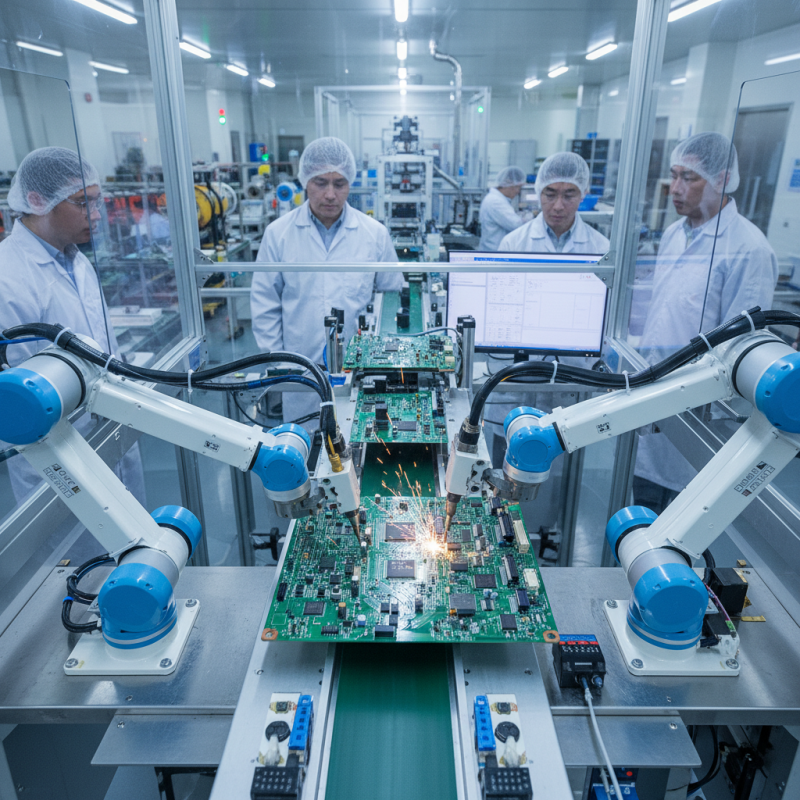
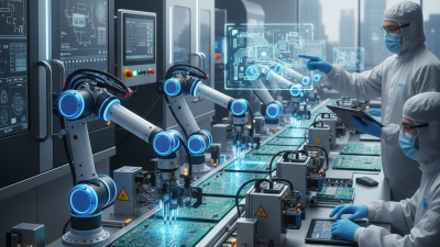
Next comes the assembly phase. Components are placed on the board and soldered into place. Some factories use automated machines, while others rely on manual labor. This part can be quite challenging. Placement accuracy is critical. A misplaced component can lead to failure in the final product. It’s a process that teaches the importance of attention to detail.
Overall, PCB assembly blends creativity with technical knowledge, making it an essential part of modern technology.
Key Components of PCB Assembly Process
The PCB assembly process is intricate and requires careful attention to detail. It involves several key components, each playing a vital role. The primary steps include PCB design, component placement, soldering, and testing. Effective design is critical. It lays the groundwork for the entire assembly process.
Designing a PCB involves software tools that allow for precise layouts. Component placement can be automated or manual. According to research from IPC, over 70% of PCB manufacturers utilize automated placement for efficiency and accuracy. This step is where components are positioned on the PCB.
Soldering is the next step, which can occur through processes like wave soldering or reflow soldering. Each process has its pros and cons. Wave soldering is quicker for bulk items, while reflow provides a clean surface mount finish. However, issues like cold solder joints can arise, which need addressing. Testing follows soldering to ensure every component functions correctly. Failure rates in this stage are typically around 5%, necessitating robust quality control measures. The complexity of this process shows the need for continuous improvement in assembly techniques.
Step-by-Step Process of PCB Assembly
PCB assembly is a detailed process that involves several stages. It begins with the design of the printed circuit board. Engineers create a blueprint containing all necessary specifications. This is critical, as errors at this stage can lead to significant issues later on. Once the design is finalized, it’s time to prepare.
Next, the PCB board is manufactured. This involves layering various materials and etching circuits. The boards are carefully drilled for components. Quality control checks happen here, but mistakes can sneak in. Some boards might not meet standards, leaving room for improvement. The final stage is component placement. Machines align components accurately, but some may misplace items. Human oversight is crucial during this stage.
After placement, soldering ensures components are secure. Automated systems often handle this, but not without risk. Some boards might experience poor solder joints. Addressing these challenges requires a dedicated workforce. The entire process is a balance of technology and human skill, making it complex yet fascinating. Continuous refinement of techniques can lead to better reliability in PCB assembly.
Common Techniques Used in PCB Assembly
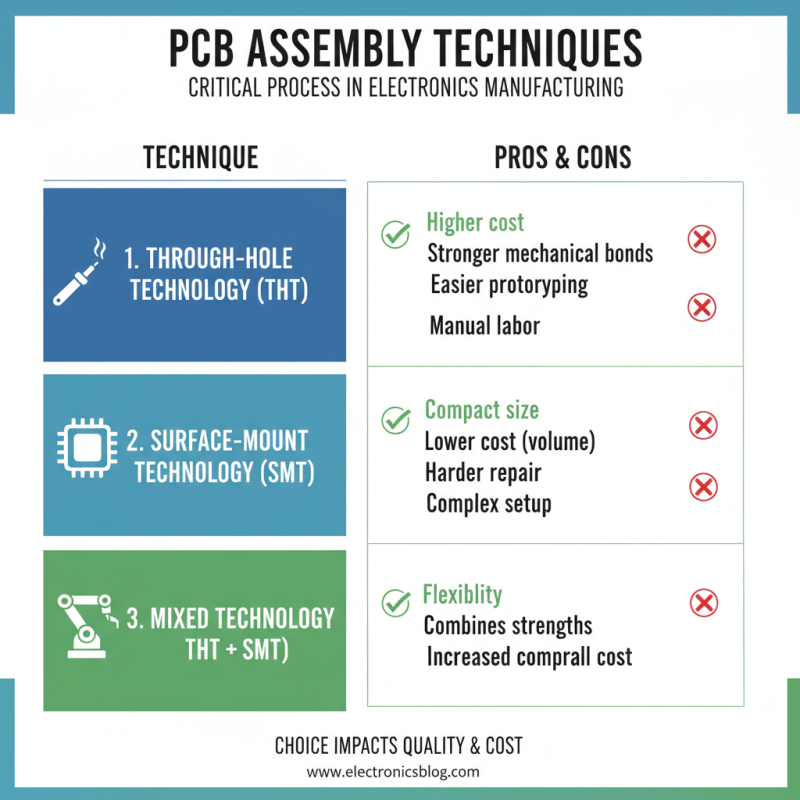
PCB assembly is a critical process in electronics manufacturing. Various techniques are used to assemble printed circuit boards (PCBs). Each technique has its pros and cons, impacting quality and cost.
Surface Mount Technology (SMT) is a widely adopted method. According to industry reports, over 80% of PCBs now use SMT. This technique allows components to be mounted directly onto the surface of the board. It leads to a more compact design and faster assembly times. However, SMT can pose challenges, such as difficulties in soldering small components.
Another common technique is Through-Hole Technology (THT). This method involves inserting component leads through holes in the PCB. Despite being less popular than SMT, THT is essential for certain components, like connectors. It provides better mechanical stability but may increase manufacturing time and costs. Balancing the use of SMT and THT requires careful consideration of the product’s needs. Each choice can influence the final performance and reliability of the PCB.
Quality Control in PCB Assembly Process
Quality control in the PCB assembly process is critical. It ensures that each printed circuit board functions as intended. Small errors can lead to significant malfunctions. Every step of the assembly process requires careful oversight.
Visual inspections are common. Operators check for solder defects, misaligned components, or foreign objects. However, this can be subjective. What one person sees, another might miss. Automated optical inspection (AOI) machines can help, but they fail sometimes. They need regular updates and adjustments to remain accurate.
Functional testing is another important aspect. Each board should be tested under real conditions. This reveals issues that visual inspections might not catch. However, testing can be time-consuming. Not every company has the resources for extensive testing. Some may skip steps, which can compromise quality. It’s a delicate balance between efficiency and thoroughness.
PCB Assembly Quality Control Metrics
This bar chart illustrates key quality control metrics in the PCB assembly process, including defect rate, assembly time, testing failures, and rework rate, helping to highlight areas for potential improvement.