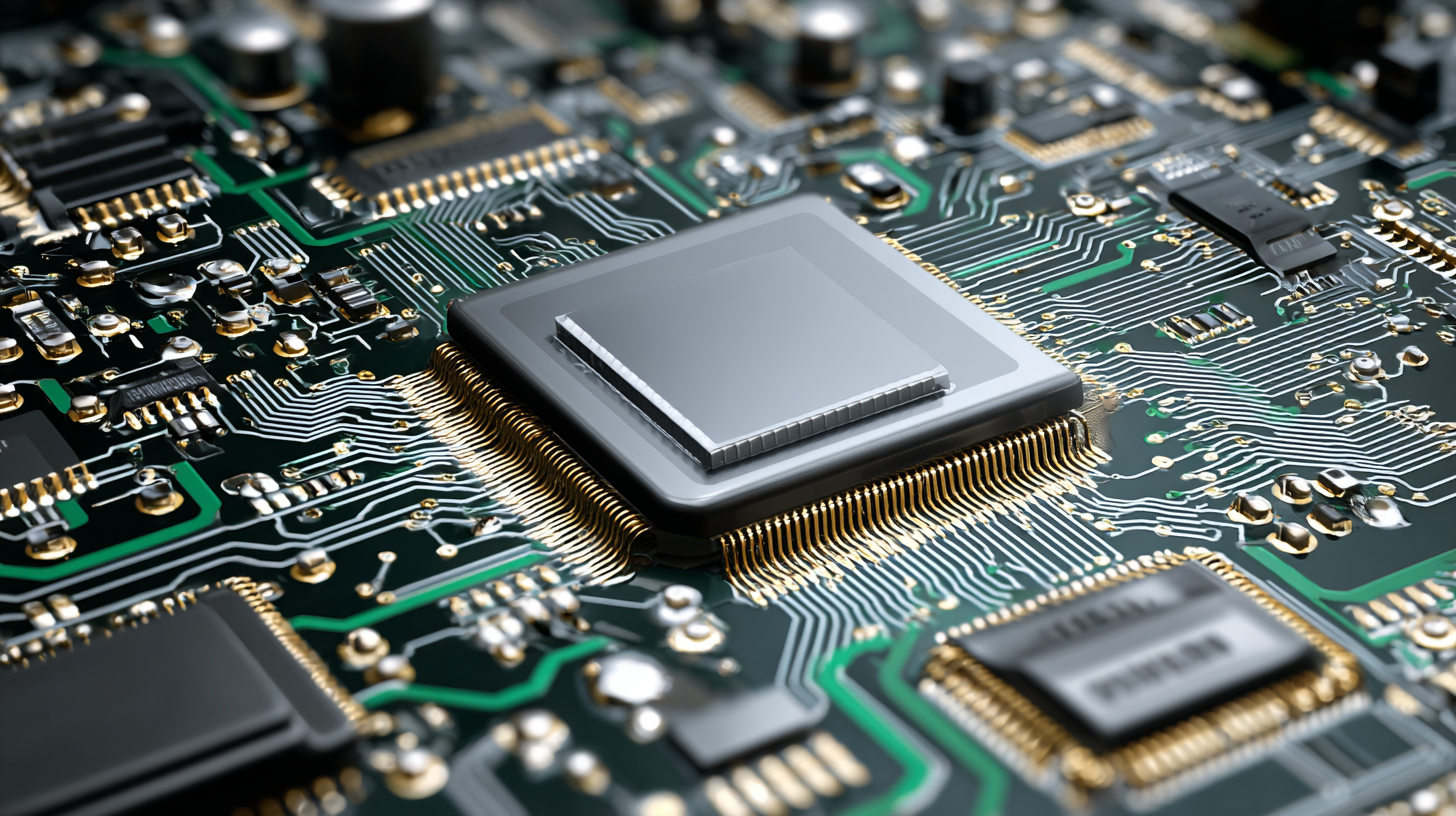
Mastering PCB Layout Techniques for Optimal Circuit Design Performance
In the rapidly evolving world of electronics, mastering PCB layout techniques is essential for achieving optimal circuit design performance. According to recent industry reports, approximately 40% of design errors can be traced back to inefficient PCB layout practices, leading to increased costs and time delays in product development. As the demand for compact and high-performing electronic devices continues to rise, engineers must prioritize PCB layout strategies that enhance signal integrity and minimize electromagnetic interference.
A well-executed PCB layout not only improves the reliability of the final product but also streamlines manufacturing processes, potentially reducing production costs by up to 30%. This article will explore effective PCB layout techniques that cater to the complexities of modern circuit design, ensuring engineers are equipped with the necessary tools to avoid common pitfalls and enhance overall performance.
Understanding the Fundamentals of PCB Layout Techniques for Enhanced Performance
Mastering PCB layout techniques is essential for enhancing the performance of circuit designs. The fundamentals of PCB layout revolve around critical aspects such as component placement, signal integrity, and thermal management. Proper component placement ensures that related components are positioned close together, minimizing trace lengths and reducing the chances of interference. This careful arrangement not only optimizes performance but also simplifies the assembly process, making it easier to troubleshoot and maintain the PCB over time.
Another crucial element of effective PCB layout is understanding and managing signal integrity. High-frequency signals can be particularly sensitive to layout techniques; thus, employing practices such as controlled impedance and differential signaling is vital. Additionally, implementing adequate grounding and power distribution strategies can mitigate noise and ensure reliable operation. Effective thermal management, including the strategic placement of heat-generating components and the use of thermal vias, further enhances circuit reliability. By mastering these fundamentals, designers can significantly improve their circuit's overall performance and longevity.
Mastering PCB Layout Techniques for Optimal Circuit Design Performance
| Technique |
Description |
Benefits |
Best Practices |
| Layer Stackup |
Selecting the right number of layers for signal integrity and power distribution. |
Improved signal integrity and reduced electromagnetic interference. |
Use a balanced stackup to minimize cross-talk. |
| Trace Width |
Determining the optimal width for power and ground traces based on current requirements. |
Ensures efficient current handling and thermal management. |
Utilize PCB design software to calculate required trace widths. |
| Ground Planes |
Using continuous ground planes to minimize noise and improve return paths. |
Reduces ground bounce and enhances signal integrity. |
Avoid splits in ground planes for sensitive signal areas. |
| Via Types |
Choosing between different via types (blind, buried, through-hole) based on design needs. |
Optimizes board space and routing efficiency. |
Use the least number of vias for critical signal paths. |
| Component Placement |
Strategically placing components for optimal signal flow and heat dissipation. |
Enhances performance and reliability of the PCB. |
Group related components together and minimize trace lengths. |
Key Design Principles for Optimizing Circuit Functionality and Reliability
When it comes to optimizing circuit functionality and reliability, several key design principles come into play. Firstly, maintaining a consistent grounding scheme is vital. Proper grounding reduces electromagnetic interference (EMI) and improves signal integrity, making the circuit more robust. This involves using a ground plane and ensuring all components are connected to it effectively. Additionally, minimizing loop areas during the design process can further decrease susceptibility to noise and crosstalk, leading to improved performance.
Another crucial aspect is the thoughtful placement of components. Strategically positioning critical parts—such as power regulators and high-frequency components—can significantly enhance circuit performance. Keeping these components close to each other while maintaining short traces minimizes inductance and resistance, fostering efficient power delivery and signal transmission. Finally, the use of appropriate trace widths and spacing reduces the risk of overheating and ensures the overall reliability of the circuit board. By adhering to these design principles, engineers can achieve not only enhanced functionality but also a higher level of reliability in their circuit designs.
PCB Layout Efficiency and Reliability Metrics
This chart illustrates the relationship between optimized PCB layout techniques and their corresponding efficiency and reliability metrics. It showcases how various design principles can significantly enhance circuit performance.
Utilizing Advanced Software Tools for PCB Design and Simulation
In the rapidly evolving field of electronics, the significance of advanced software tools for PCB design and simulation cannot be overstated. A recent industry report highlights that approximately 80% of engineers utilize specialized PCB software to streamline their design processes. This shift towards digital design environments has led to a notable reduction in time-to-market, with some companies reporting a 30% faster product development cycle by effectively leveraging these tools.
Moreover, modern simulation capabilities integrated into PCB design software enable engineers to perform real-time analysis of electrical performance and thermal management, enhancing the reliability of circuit designs. According to a study by the IPC, firms employing advanced simulation technologies can reduce prototyping costs by as much as 40%, as potential issues can be identified and resolved during the design phase rather than post-production.
As the complexity of electronic systems continues to increase, mastering these sophisticated software solutions becomes essential for engineers looking to achieve optimal circuit performance and ensure product quality.
Best Practices for Component Placement and Routing in PCB Layout
Component placement and routing are fundamental aspects of PCB layout that directly influence circuit performance. Best practices for component placement involve strategic positioning that minimizes signal path lengths, reducing potential delay and interference. Prioritizing the arrangement of high-speed components close to their respective connectors or interfaces helps maintain signal integrity. Moreover, organized placement ensures effective thermal management, allowing heat-sensitive components to operate within their optimal temperature ranges, thereby enhancing reliability.
Routing, on the other hand, demands attention to both trace width and spacing. Adequate trace dimensions can prevent overheating and ensure the circuit can handle the required current without degradation. Additionally, using automated routing tools can facilitate efficient and precise trace routing, minimizing the risk of errors commonly associated with manual processes. The integration of AI in PCB design is becoming increasingly vital, as advanced algorithms can optimize routing paths and component placement, ultimately leading to improved performance and faster design cycles. By leveraging these best practices in conjunction with cutting-edge technology, designers can achieve superior circuit functionality.
Common Pitfalls in PCB Design and How to Avoid Them for Better Outcomes
When it comes to PCB design, many engineers fall victim to common pitfalls that can compromise the overall performance of their circuits. One prevalent issue is neglecting proper grounding techniques. Inadequate grounding can lead to noise and interference, adversely affecting signal integrity. To avoid this, designers should prioritize a solid ground plane and strategically place vias to minimize loop areas, ensuring a stable reference for all signals.
Another frequent mistake involves improper component placement. Placing components without considering their interaction and the signal paths can introduce unwanted parasitic effects and increase electromagnetic interference. A well-thought-out layout should group related components together, keeping high-speed signals short and direct. Furthermore, designers should pay attention to the thermal management of high-power components, ensuring adequate spacing and thermal vias to dissipate heat effectively. By being mindful of these pitfalls and employing thoughtful design strategies, engineers can significantly enhance the performance of their PCB designs.