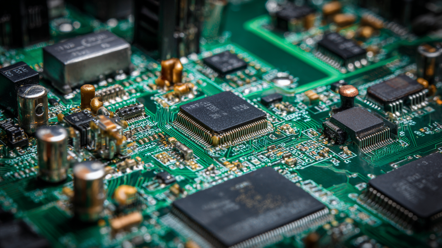
The Evolution of PCB Assembly Techniques Transforming Modern Electronics
The progression of technology has dramatically influenced the manufacturing processes within the electronics industry, particularly in the realm of PCB assembly. As the demand for more compact, efficient, and reliable electronic devices continues to rise, innovative assembly techniques have emerged, transforming the way printed circuit boards are produced and integrated into final products. This evolution encompasses a variety of methods and technologies, including surface-mount technology (SMT), through-hole assembly, and advanced automated systems, each offering unique advantages that cater to different applications. By examining the latest trends and advancements in PCB assembly, we can gain a clearer understanding of how these techniques not only enhance performance but also drive the future of modern electronics, making them more accessible and effective for consumers across the globe.
The Historical Journey of PCB Assembly Techniques in Electronics
The evolution of PCB assembly techniques has been a pivotal journey in the advancement of electronics. Early in the 20th century, printed circuit boards (PCBs) began as simple designs, primarily utilizing wire and point-to-point assembly. Craftsmen manually connected components, which was not only time-consuming but also prone to errors. The introduction of photolithography in the late 1950s marked a significant breakthrough, enabling more intricate circuit designs. This innovation paved the way for greater miniaturization and reliability in electronic devices.
As technology continued to advance, the 1980s witnessed the arrival of surface mount technology (SMT), which revolutionized PCB assembly. SMT allowed for smaller components to be mounted directly onto the surface of the board, vastly improving density and performance. Coupled with automated assembly processes, manufacturers could achieve higher speeds and lower production costs. The subsequent integration of computer-aided design (CAD) and robotic assembly systems further transformed PCB assembly, leading to today’s high-tech electronics that power everything from smartphones to sophisticated medical devices. This historical journey highlights the significant milestones that have shaped the modern electronics landscape.
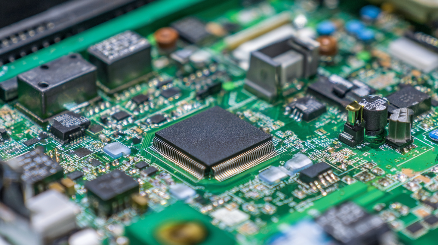
Key Innovations Revolutionizing PCB Fabrication in the 21st Century
The landscape of printed circuit board (PCB) assembly techniques is undergoing a profound transformation in the 21st century, driven by key innovations that enhance efficiency and functionality. One notable development is the integration of nanotechnology into PCB manufacturing. This technology enables the creation of lighter and stronger materials, which not only reduces the weight of electronic devices but also improves their durability. Additionally, the application of nanosensors is paving the way for more sophisticated monitoring capabilities within PCBs, which can help pinpoint failures or performance issues in real-time.
Another significant innovation lies in the advent of advanced 3D printing techniques for PCB fabrication. This method allows for rapid prototyping and customized designs, enabling manufacturers to produce complex circuits with greater precision than traditional methods. The evolution of these techniques reflects a broader trend in the electronics industry, where flexibility and speed are becoming increasingly essential. As companies adapt to these trends, the synergy between advanced manufacturing methods and the growing demand for high-performance electronics continues to reshape the future of PCB assembly.
The Evolution of PCB Assembly Techniques
Automation and Robotics: The Game Changers in PCB Assembly
The transformation of PCB assembly techniques has been significantly influenced by advancements in automation and robotics. These technologies have reshaped traditional manufacturing processes, leading to increased efficiency and precision in producing printed circuit boards. Automated systems can reliably handle complex tasks such as component placement, soldering, and inspection, minimizing human error and reducing production time. This has enabled manufacturers to meet the rising demand for high-quality electronics while maintaining competitive pricing.
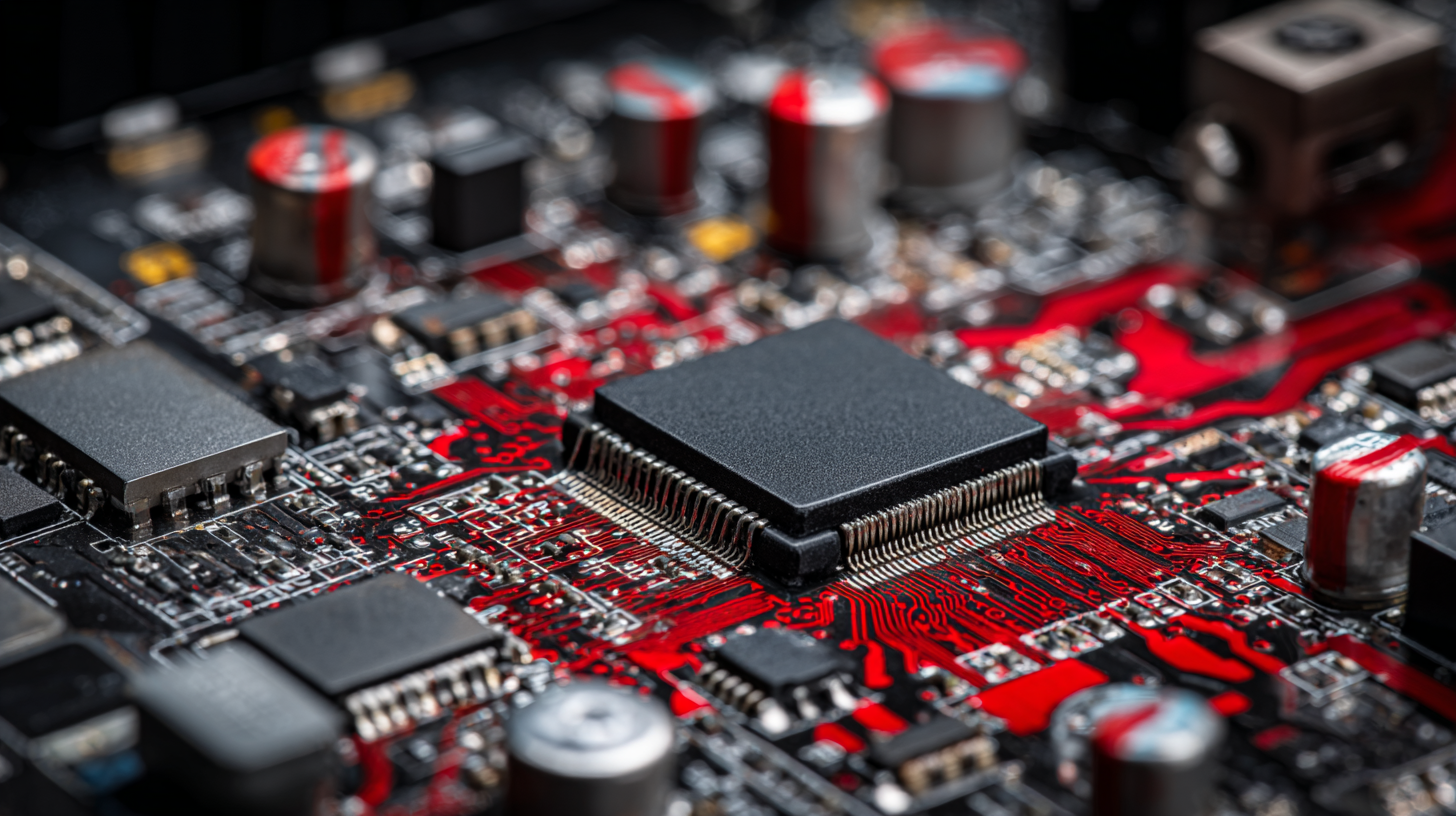 Robotics, in particular, have taken PCB assembly to the next level by introducing flexibility and adaptability within production lines. Modern robotic arms equipped with artificial intelligence can quickly adjust to different PCB designs, allowing for rapid prototyping and small-batch production without sacrificing quality. Moreover, these robots can operate continuously, increasing throughput and enabling manufacturers to scale operations in response to market trends. As the electronics industry continues to evolve, the integration of automation and robotics will undoubtedly remain a pivotal factor in driving innovation within PCB assembly techniques.
Sustainability in PCB Assembly: Eco-Friendly Practices and Materials
Sustainability has become a critical focus in PCB assembly, where eco-friendly practices and materials are increasingly prioritized to reduce environmental impact. Manufacturers are exploring lightweight materials such as bioplastics and recycled substrates, which not only lessen waste but also minimize energy consumption during production. These innovative materials offer comparable performance to traditional options while promoting a circular economy and lowering the carbon footprint of electronic devices.
Additionally, sustainable practices in PCB assembly involve optimizing production processes to conserve resources. Techniques such as selective soldering, which reduces the use of solder materials, and advanced automation can lead to significant energy savings. Moreover, waste management initiatives are being implemented to recycle electronic components, preventing hazardous materials from ending up in landfills. By embracing these eco-conscious strategies, the electronics industry is not only enhancing its sustainability profile but also responding to consumer demand for greener products.
The Evolution of PCB Assembly Techniques Transforming Modern Electronics - Sustainability in PCB Assembly: Eco-Friendly Practices and Materials
| Technique |
Description |
Eco-Friendly Materials |
Benefits |
| Surface Mount Technology (SMT) |
A method that mounts components directly onto the surface of PCBs, allowing for higher component density. |
Lead-free solder |
Reduced waste and more compact design. |
| Through-Hole Assembly |
Traditional technique where components are placed in holes and soldered on the other side. |
Biodegradable adhesives |
Greater durability and easier recycling. |
| Flexible PCB Assembly |
Involves the use of flexible substrates to create light and compact designs. |
Non-toxic polyimide substrates |
Enhanced design versatility and waste reduction. |
| Robotic Automation |
Utilizes robots for assembly, which increases precision and efficiency. |
Recyclable materials in robotic parts |
Lower energy consumption and reduced error rates. |
| 3D Printing |
Additive manufacturing technique that reduces material waste. |
Bioplastic filaments |
Less waste generated and rapid prototyping capabilities. |
Future Trends in PCB Assembly: What to Expect in the Next Decade
The landscape of PCB assembly is rapidly evolving, driven by technological advancements and increasing demand for more efficient manufacturing processes. In the next decade, we can expect the industry to embrace automation and artificial intelligence to enhance precision and efficiency. Machine learning algorithms will play a crucial role in optimizing assembly lines, enabling real-time data analysis to predict defects and minimize waste. As robots become more sophisticated, they will take over repetitive tasks, allowing human workers to focus on complex problem-solving and design improvements.
Another significant trend will be the rise of modular PCB assembly techniques. This approach allows manufacturers to produce smaller, more flexible circuit boards that can be easily adapted for various applications. With the growth of the Internet of Things (IoT) and wearable technology, the demand for customized, compact PCBs will surge. Furthermore, advancements in materials science will lead to the development of new substrates that offer better performance in diverse environments, expanding the possibilities for electronic devices.
As these trends unfold, the future of PCB assembly promises to be innovative and responsive to the ever-changing needs of the electronics market.