Understanding the Essential Steps in Creating a High Quality PCB Prototype
In the electronics industry, the demand for high-quality PCB prototypes has surged, reflecting the critical role they play in product development and innovation. According to a recent industry report by Research and Markets, the global PCB prototype market is expected to reach $2.5 billion by 2025, with a CAGR of 10% from 2020 to 2025. This highlights the increasing importance of rapid prototyping, where companies are striving to reduce time-to-market while ensuring superior quality and performance.
Creating a PCB prototype involves a meticulous process that incorporates advanced design techniques, precise manufacturing, and rigorous testing protocols. By understanding the essential steps in this process, manufacturers can not only enhance the reliability and functionality of their products but also maintain a competitive edge in an ever-evolving marketplace.
Key Considerations in PCB Design: Choosing the Right Materials and Components
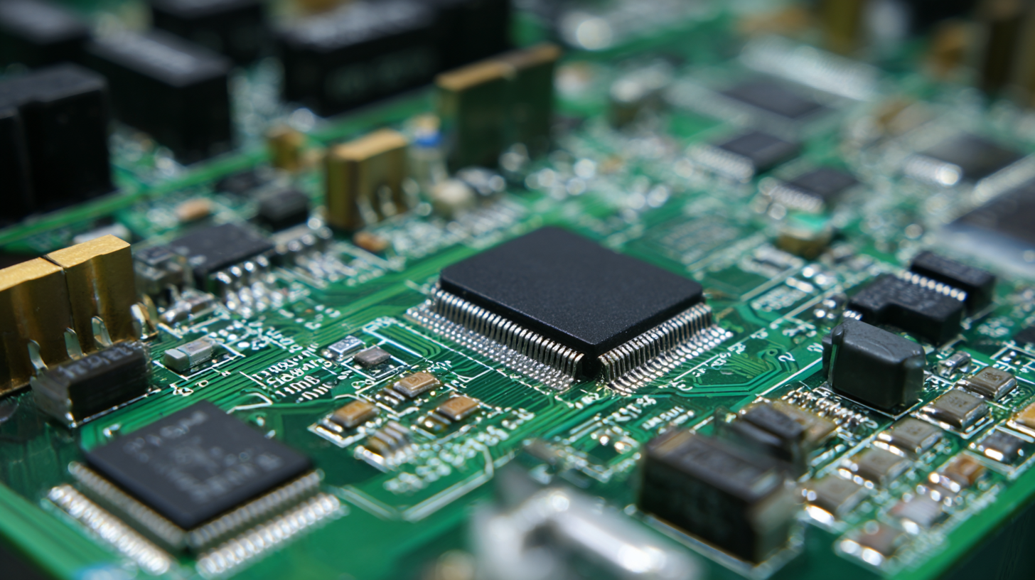
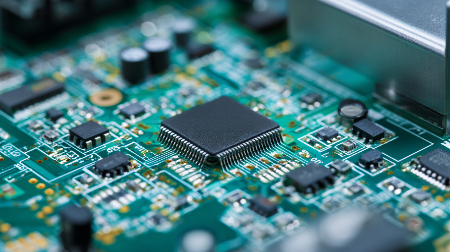
When designing a printed circuit board (PCB) prototype, one of the most crucial factors to consider is the selection of materials and components. The choice of substrate material plays a significant role in the PCB's overall performance, affecting factors such as thermal conductivity, signal integrity, and durability. Common materials like FR-4, a fiberglass epoxy, are widely used due to their balance of cost and performance, but for high-frequency applications, materials like Rogers or Teflon may be required to minimize signal loss and improve efficiency.
In addition to the substrate, the selection of components is equally important. Designers must focus on choosing components that not only meet functional requirements but also align with the PCB's design specifications. Factors such as size, power rating, and operating temperature must be carefully evaluated to ensure compatibility and reliability. Furthermore, understanding the interconnectivity between components is essential, as it can impact the PCB's layout and functionality. By prioritizing material and component selection, designers can create high-quality PCB prototypes that meet both technical and performance standards.
Understanding the Essential Steps in Creating a High Quality PCB Prototype
Importance of Design Software in Optimizing PCB Prototyping Efficiency
The role of design software in PCB prototyping cannot be overstated, as it significantly enhances efficiency and accuracy throughout the development process. Advanced design tools provide engineers with an array of features that streamline the creation of complex circuit layouts. These tools often include automatic routing capabilities, real-time design rule checks, and visualization options, which help in identifying potential issues before moving to fabrication. By employing such software, designers can iterate quickly, minimizing the time spent on revisions and reducing the number of prototypes needed.
Moreover, effective design software facilitates collaboration among team members, regardless of their geographical locations. Cloud-based solutions allow for simultaneous access to projects, enabling team members to contribute to the design process in real-time. This interconnectedness not only speeds up development timelines but also ensures that all stakeholders are aligned with the project's goals. The integration of simulation tools within the software further allows for testing and validation of designs before they reach production, ensuring that the final prototype will meet specifications and function as intended.
Common Challenges in PCB Prototyping and How to Overcome Them
In the realm of PCB prototyping, several common challenges can hinder the development process. One frequent issue is design errors that can lead to functional failures during testing. To combat this, it's essential to implement a robust review process involving multiple team members who can provide fresh insights. Additionally, utilizing design software with built-in error-checking functions can help catch mistakes early in the design phase.
Another challenge is material and component sourcing. Delays in obtaining high-quality components can stall prototyping efforts. To mitigate this, develop relationships with reliable suppliers and consider using alternative parts that are readily available. Also, maintaining an organized inventory can help ensure you have essential components on hand when needed.
**Tips:** When designing PCBs, always include test points for easier debugging. Moreover, keep your prototypes simple; focus on validating the core functionalities before adding complexity. This approach not only facilitates quicker testing but also helps identify design flaws quickly.
Testing and Validation: Ensuring High Quality PCB Prototype Performance
Testing and validation are critical components in the development of a high-quality PCB prototype, as they ensure the final product operates reliably under real-world conditions. According to a report by IPC, an international trade association, nearly 30% of PCB prototypes fail to meet their performance specifications during initial testing phases. This emphasizes the importance of rigorous testing processes, which can include both electrical and thermal evaluations to identify potential failures that may not be apparent during the design phase.
One effective approach to ensuring a PCB's performance is the implementation of Design for Testability (DFT) techniques. Research from the IEEE indicates that incorporating DFT in the design stage can reduce testing time by upwards of 50%, significantly minimizing time-to-market while enhancing the reliability of the final product. By utilizing automated testing equipment and establishing comprehensive validation protocols, designers can catch anomalies early, ensuring that the prototype meets both quality standards and functional expectations before full-scale production. These steps not only enhance prototype quality but also contribute to cost efficiencies and better overall project outcomes.
Cost Analysis: Budgeting for High-Quality PCB Prototyping and Production
When budgeting for high-quality PCB prototyping and production, a detailed cost analysis is essential. The primary expenses include material costs, manufacturing processes, and design complexity. High-grade materials, such as FR-4, and advanced features like multi-layer designs significantly increase costs. Additionally, sourcing components and ensuring their reliability is vital, as using low-quality parts can compromise the overall performance and longevity of the PCB.
Moreover, production methods also impact the budget. Traditional methods may be more affordable but might not deliver the precision required for complex designs. Conversely, investing in advanced manufacturing techniques, like laser engraving and automated assembly, can lead to higher upfront costs but often result in improved yield rates and quicker turnaround times. By evaluating these factors, engineers can make informed decisions on allocating their budget effectively, ensuring that they achieve a balance between quality and cost-efficiency in their PCB projects.
Understanding the Essential Steps in Creating a High Quality PCB Prototype - Cost Analysis: Budgeting for High-Quality PCB Prototyping and Production
| Cost Component |
Estimated Cost ($) |
Description |
| PCB Design Fees |
500 |
Cost for hiring a PCB designer or using design software. |
| Materials Costs |
300 |
Costs associated with substrates, copper, solder mask, etc. |
| Manufacturing Costs |
800 |
Fees for the actual production of the PCB prototypes. |
| Testing and Validation |
200 |
Cost for quality control and functional testing of prototypes. |
| Shipping and Handling |
100 |
Costs to ship the prototypes to the development team. |
| Total Estimated Cost |
2000 |
|