10 Best Tips for Efficient PCB Printing Techniques?
In the world of electronics, mastering PCB printing is essential. High-quality printed circuit boards are vital for device performance. However, achieving efficiency in PCB printing can be challenging. Many factors influence the process, from design to material selection.
Understanding these factors can greatly enhance productivity and reduce costs. Are you using the right printing techniques? This question can define the success of your project. Often, the simplest adjustments lead to better results. Small mistakes can sometimes result in significant delays. Recognizing common pitfalls is crucial for improvement.
Professionals in the field have learned through experience. They often reflect on their methods and make necessary adjustments. Each day offers new lessons in enhancing PCB printing techniques. Embracing this journey ensures that your printed circuit boards meet industry standards and perform reliably.
Understanding the Basics of PCB Printing Techniques
Understanding the basics of PCB printing techniques is crucial for creating effective circuit boards. The process begins with designing your PCB layout. This is where you determine the placement of components and traces. A well-organized design prevents future errors. Attention to detail in this phase is vital. Mistakes can be costly.
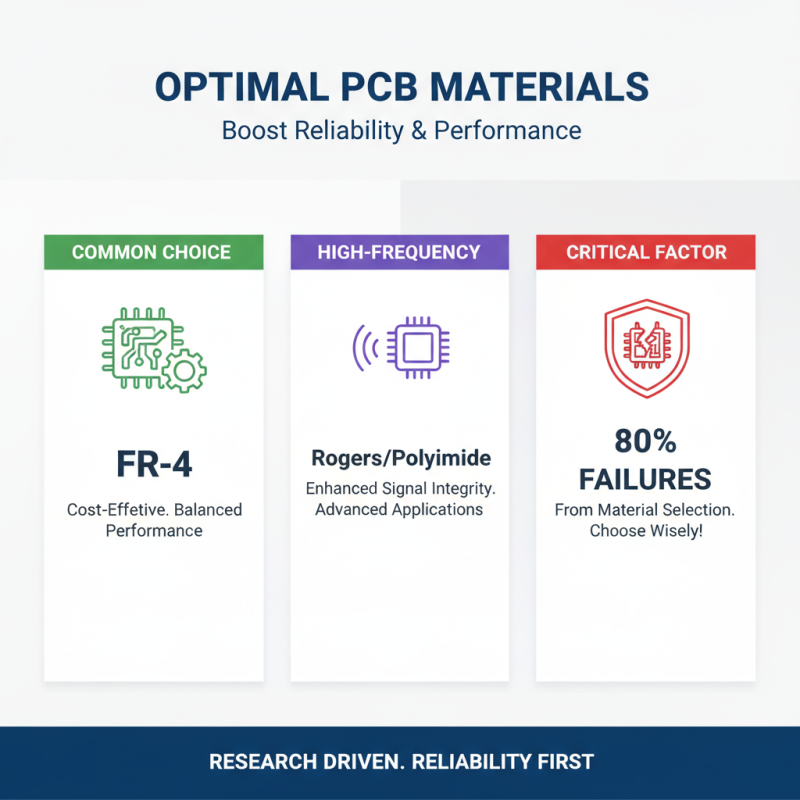
When it comes to printing, the choice of materials matters. Different substrates can yield varying results. It's worth experimenting with several types. Some may provide better adhesion, while others might be more flexible. However, this can lead to confusion if not clearly documented. Always assess the compatibility of inks with your chosen substrate.
Lastly, the calibration of printing equipment requires careful consideration. Even minor adjustments can change the outcome. Inconsistent pressure or misalignment often results in defects. Regular maintenance is necessary but can be overlooked. Keeping a checklist helps ensure all steps are followed. Each mistake offers valuable lessons for the next project. Embrace the learning process to improve your skills.
Optimizing PCB Design for Printing Efficiency
When optimizing PCB design for printing efficiency, one must focus on several key factors. Efficient layout reduces material waste and ensures better print quality. High-density designs might seem appealing, but they can complicate the printing process. Simplifying designs often leads to more successful prints.
Select suitable trace widths. Narrow traces can save space but might be challenging for printing. Wider traces offer reliability during the printing process. Test various widths to find the best balance for your projects. It's an iterative process, and you might face some challenges.
Incorporate proper pad designs. Incorrect pad sizes can lead to poor soldering and component placement. Use standard sizes as guidelines. This can enhance the overall print quality. Remember, a design’s efficiency is key, but don’t overlook the potential issues that might arise from overly ambitious layouts. Reflecting on past designs will guide you in making better decisions.
10 Best Tips for Efficient PCB Printing Techniques
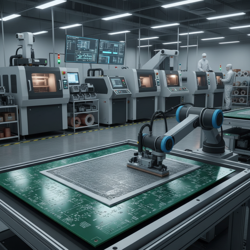
Utilizing Advanced Printing Technologies for Better Results
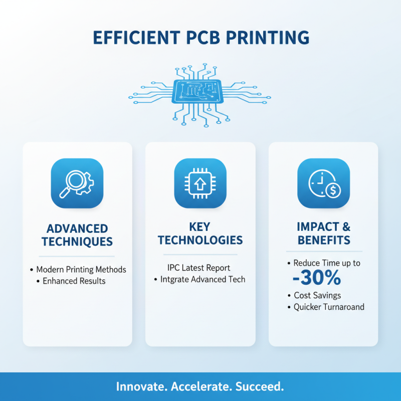
Efficient PCB printing requires advanced techniques and technologies. Utilizing modern printing methods can drastically enhance results. According to the IPC’s latest report, incorporating advanced technologies can reduce production time by up to 30%. This efficiency translates into cost savings and quicker turnaround times.
One effective tip is to optimize print settings. Adjusting the layer thickness and speed can impact precision. For example, using a smaller layer height can improve detail, but it may slow down the process. Finding the right balance is essential. Many engineers often overlook this aspect.
Another key factor is ink quality. High-quality inks provide better adhesion and durability. Poor-quality inks can lead to flaws that compromise the functionality of PCBs. Regularly testing inks is crucial. There's always room for improvement. Sometimes, switching suppliers can yield better results. It’s a continuous learning process in the industry, driven by technological advancements and market demands.
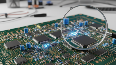
Effective Post-Processing Methods for PCB Quality Improvement
Effective post-processing methods can significantly enhance the quality of printed circuit boards (PCBs).
At this stage, it’s essential to assess the imperfections left from printing. According to recent
industry reports, nearly 30% of PCB defects stem from inadequate
post-processing steps. This highlights the need for thorough techniques to ensure top-notch results.
One key tip is to adopt efficient cleaning methods. Residual inks or chemicals can lead to reliability
issues later. Cleaning with ultrasonic or solvent-based techniques can remove these contaminants
effectively. Another critical aspect is the curing process. Proper heat treatment can improve the adhesion
of printed components. Industry data shows that curing errors can lead to a 25%
decrease in performance reliability.
Lastly, consider implementing additional inspections post-processing. Automated optical inspection (AOI)
systems can catch errors that manual inspections may miss. This can help in reinforcing the overall quality
of the PCBs. Focusing on these methods not only increases reliability but also reduces waste and production
costs in the long term. Regular reflections on these processes can lead to continuous improvement.