Best 10 PCB Layout Tips for Optimizing Your Design Efficiency and Performance
When it comes to designing high-performance electronic circuits, the importance of an efficient PCB layout cannot be overstated. Industry expert Dr. Maryann W. Hannon, a leading authority on PCB design, once remarked, “A meticulous PCB layout is the cornerstone of successful electronic design, influencing performance, reliability, and manufacturability.” As the demand for increasingly compact and complex electronics grows, optimizing PCB layout becomes not just a best practice but a necessity for engineers striving to meet these challenges.
In this article, we will explore the best 10 tips for optimizing your PCB layout, which will enhance both your design efficiency and the performance of your final product. By implementing these strategies, designers can minimize issues such as signal interference, thermal management, and manufacturing complexities. Whether you are a seasoned professional or a newcomer to the field, these insights will guide you towards creating superior PCB layouts that meet the evolving demands of the industry. Join us as we delve into practical techniques that can elevate your design and push the boundaries of what is achievable in the world of electronics.

Essential Design Principles for Effective PCB Layout
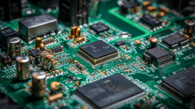
Effective PCB layout is crucial for achieving optimal performance and reliability in electronic designs. One essential principle is to maintain a proper trace width to ensure adequate current handling. This not only prevents overheating but also minimizes voltage drops across connections. When designing traces, it's important to consider the total current that will pass through them and select widths accordingly using appropriate standards or calculators.
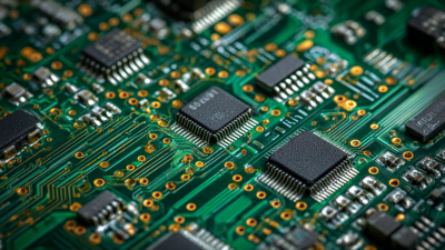
Another fundamental aspect of PCB layout is the strategic placement of components. Grouping related components together helps reduce the length of signal paths and minimizes interference. Additionally, placing decoupling capacitors close to the power pins of ICs ensures stable voltage supply and reduces power noise. Furthermore, maintaining a balanced ground plane improves signal integrity and reduces electromagnetic interference, which is crucial for high-speed designs. By following these principles, designers can significantly enhance their PCB layout efficiency and overall product performance.
Techniques for Reducing Signal Interference in PCB Designs
Reducing signal interference in PCB designs is crucial for enhancing both performance and reliability. One of the most effective techniques is to maintain proper trace spacing. Ensure that traces carrying high-frequency signals are adequately separated from those carrying lower-frequency signals. This can significantly minimize crosstalk and maintain signal integrity.
Another essential tip is to use ground planes effectively. By incorporating a solid ground plane in your PCB layout, you can create a low-impedance reference, which helps to reduce electromagnetic interference (EMI). Additionally, placing sensitive components close to the ground plane will improve performance by shielding them from noise.
Lastly, implementing differential signaling can also mitigate signal interference. By using twisted pairs for high-speed signals, you can reduce electromagnetic radiation and susceptibility to noise. This technique ensures that any interference affects both wires equally, thereby maintaining the integrity of the transmitted signal. By applying these design tips, you can optimize your PCB layout for superior efficiency and performance.
Optimal Component Placement for Enhanced Performance
Optimal component placement is crucial for enhancing the performance of your PCB design. When components are strategically arranged, it can lead to reduced signal interference and better thermal management. Begin by identifying critical signal paths and placing high-speed components closer together to minimize the trace lengths. This approach not only optimizes performance but also simplifies the routing process, making it easier to manage potential issues that could arise from excessive distances between components.
Another important tip is to consider the power distribution network (PDN) when placing components. Ensure that power-hungry components are located near the power supply to minimize voltage drop and improve efficiency. Additionally, grouping related components can help reduce the complexity of the layout. For instance, placing all analog components in one area and digital components in another can help avoid interference and enhance overall performance. Keep in mind that adequate spacing and thoughtful organization will ultimately lead to a more efficient and effective PCB layout.
Best 10 PCB Layout Tips for Optimizing Your Design Efficiency and Performance
Best Practices for Layer Management in PCB Layouts
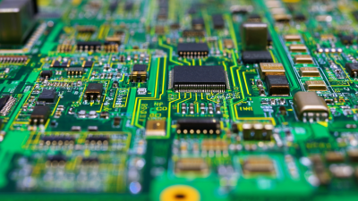
 When it comes to optimizing PCB layouts, effective layer management is crucial for enhancing both design efficiency and overall performance. Organizing layers thoughtfully can minimize electromagnetic interference and improve signal integrity, which is especially important in RF and high-speed digital designs. Utilizing well-defined stackups can not only streamline the layout process but also facilitate better thermal management and component placement.
In light of recent advancements in PCB technology, such as the ability to quickly create 3D printed circuit boards, the importance of layer management becomes even more pronounced. The rapid production capabilities complement the need for efficient layouts, allowing designers to experiment with new configurations without the lengthy lead times typically associated with traditional manufacturing methods.
As PCB design software evolves, features that enhance synchronous team collaboration and automated routing make effective layer management accessible to more designers, further improving overall design processes and outcomes.
Tools and Software to Boost Your PCB Design Workflow
In the realm of PCB design, leveraging the right tools and software can significantly enhance workflow efficiency and optimize overall performance. According to a recent industry report by IPC, organizations that integrate advanced PCB design tools can reduce their time-to-market by up to 30%. This is particularly critical in fast-paced sectors like consumer electronics and automotive, where the pressure to innovate quickly is relentless.
Software solutions like Altium Designer and Autodesk Eagle provide robust simulation features that allow designers to visualize and resolve potential issues before physical prototyping, thus streamlining the development process.
Moreover, a study by the Electronics Industry Association reveals that using integrated design environments can decrease error rates by as much as 40%. Tools that offer real-time collaboration and revisions, such as KiCad and Creo, empower teams to work cohesively, facilitating communication and project management.
With a well-chosen set of tools, designers can not only improve their design speed but also enhance the fidelity of their work, ensuring higher quality PCBs that meet stringent industry standards. The right software is thus essential for manufacturers aiming to maintain a competitive edge in an increasingly complex market.