Understanding the Advances in PCB Assembly Techniques for Modern Electronics
The rapid evolution of technology in the electronics sector has necessitated significant advancements in
PCB assembly techniques, making it a crucial topic
for engineers and manufacturers alike. As the demand for smaller, more efficient, and highly integrated
electronic devices grows, understanding the methodologies and innovations in PCB assembly becomes imperative.
This essay delves into the cutting-edge techniques revolutionizing the PCB assembly process, addressing
aspects such as automation,
material selection, and
design intricacies that contribute to enhanced performance and reliability.
By examining the landscape of modern electronics, we aim to highlight how these advancements in PCB assembly
not only streamline production but also ensure that electronic devices meet the
increasing complexity and
functionality required by today's consumers.
Through this exploration, we will uncover the pivotal role that innovative PCB assembly practices play
in shaping the future of electronics.
Advancements in Soldering Technologies for Improved PCB Assembly Efficiency
 Advancements in soldering technologies are crucial in enhancing PCB assembly efficiency, particularly in the context of modern electronics. As the electronics industry evolves, manufacturers are increasingly relying on advanced soldering techniques, such as selective soldering and reflow soldering, to meet the growing demand for high-quality and reliable PCB assemblies. According to a recent industry report from IPC, the global market for soldering equipment is expected to grow at a CAGR of 7.2% from 2022 to 2027, emphasizing the vital role that innovative soldering solutions play in the production process.
For manufacturers aiming to optimize their PCB assembly, adopting automated soldering processes can significantly reduce errors and increase throughput. For instance, robotic soldering systems can achieve a degree of precision and repeatability that is difficult to match with manual methods. Additionally, the introduction of lead-free solders has resulted in better thermal stability and improved solder joint reliability, addressing environmental regulations and consumer demands for safer materials.
Tips: When selecting a soldering method, consideration should be given to the complexity of the assembly and the types of components used. Regular maintenance of soldering equipment is essential to sustain performance levels and to avoid downtime. Furthermore, investing in workforce training on the latest soldering techniques can enhance quality and efficiency on the production line.
The Role of Automation in Modern PCB Assembly Processes
The integration of automation in modern PCB assembly processes is revolutionizing the electronics manufacturing landscape. As outlined in recent industry reports, the automation in electronic manufacturing services (EMS) market is expected to see significant growth, with a focus on advanced technologies like robotics and artificial intelligence. By 2034, it's projected that the value of this market will reach unprecedented heights, driven by the increasing demand for efficiency and cost savings. Through the implementation of automated systems, manufacturers can enhance production rates and utilize materials more effectively, leading to improved overall productivity.
Moreover, automated PCB manufacturing is breaking new ground, allowing engineers to push the boundaries of design complexity and innovation. Implementing automated calibration systems enhances measurement accuracy, significantly reducing reliance on manual processes. This transformation is further supported by AI technologies, which facilitate sophisticated design applications and optimize manufacturing workflows. As the electronics industry continues to evolve, the synergy between automation and PCB assembly processes will be crucial in meeting the demands of modern electronics and shaping the future of manufacturing.
Advances in PCB Assembly Techniques - Automation Impact
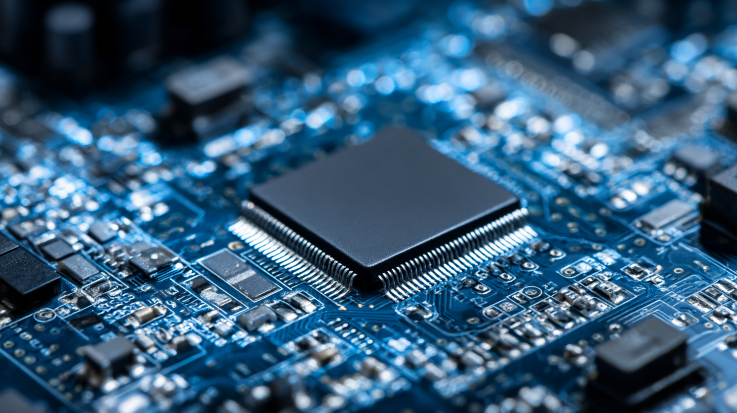
Innovative Materials for Enhanced Durability and Performance in PCBs
Innovative materials play a crucial role in enhancing the durability and performance of printed circuit boards (PCBs). According to a report by MarketsandMarkets, the global PCB market is expected to reach USD 68.69 billion by 2025, driven largely by innovations in material science. Traditional materials like FR-4 are being supplemented or replaced by high-performance laminates and ceramics that offer improved thermal stability and electrical performance. For instance, liquid crystal polymer (LCP) and polyimide materials provide significant enhancements in flexibility and resistance to extreme temperatures, making them ideal for high-reliability applications in sectors like aerospace and telecommunications.
**Tip:** When selecting PCB materials, consider their thermal conductivity and thermal expansion coefficients. Materials with lower thermal expansion rates reduce the risk of cracking and delamination in multilayer designs.
Additionally, advancements in conductive materials have paved the way for improved signal integrity and reduced electromagnetic interference (EMI). Reports indicate that using advanced copper alternatives, such as silver or hybrid conductive inks, can significantly enhance the electrical performance of PCBs. This is particularly important in applications requiring high-speed data transfer, where even the slightest performance limitation can lead to failure.
**Tip:** Explore the benefits of using nanomaterials in PCB design. Incorporating carbon nanotubes or graphene may offer superior conductivity while minimizing weight and thickness, crucial for modern compact electronics.
Eco-friendly Practices in PCB Manufacturing and Assembly Techniques
Eco-friendly practices in PCB manufacturing and assembly are becoming increasingly crucial as the electronics industry seeks to minimize its environmental impact. Current initiatives have begun to prioritize sustainable materials and processes over mere compliance with regulations. This shift reflects a growing recognition of the need for responsible practices that address not only efficiency but also ecological stewardship. Eco-friendly materials such as biodegradable substrates and lead-free soldering techniques are gaining traction, helping to reduce the carbon footprint of PCB production.
Moreover, advancements in technology are driving innovative approaches in this domain. For instance, methods like using aerial robotics are being explored to enhance construction and assembly processes while ensuring sustainability. These technologies promise not only to streamline operations but also to mitigate risks associated with traditional methods. In parallel, the rise of transparent and flexible electronics hints at the future of sustainable design, emphasizing both functionality and aesthetic considerations. As the industry evolves, integrating these eco-friendly practices into PCB assembly techniques will play a pivotal role in shaping sustainable electronic manufacturing.
Future Trends in PCB Assembly: Smart Technologies and Industry 4.0 Integration
The integration of smart technologies within PCB assembly processes is transforming modern electronics manufacturing. As industries adopt Industry 4.0 principles, which emphasize automation and real-time data exchange, we are witnessing a significant shift in manufacturing efficiency and precision. A recent report forecasts that the smart manufacturing market will exceed USD 600 billion by 2030, driven by advancements in IoT and AI technologies. These innovations not only streamline production but also enable customized manufacturing solutions tailored to specific customer needs.
In the automotive sector, the influence of AI is particularly profound, with manufacturers leveraging data analytics to optimize their workflows, resulting in enhanced operational efficiencies. As the automotive industry embraces automation, experts predict that the factory automation market could reach USD 370 billion by 2034, growing at a CAGR of 6.5%. Cutting-edge developments, including bio-microsystem integration and Lab-on-PCB technologies, further illustrate how smart manufacturing is reshaping the landscape. This evolution underscores the importance of staying abreast of these trends to remain competitive and innovative in the rapidly changing electronics market.
Understanding the Advances in PCB Assembly Techniques for Modern Electronics - Future Trends in PCB Assembly: Smart Technologies and Industry 4.0 Integration
| Technique |
Description |
Benefits |
Future Trends |
| Automated Optical Inspection (AOI) |
A process that uses visual methods to inspect and ensure the quality of PCB assemblies. |
Increased accuracy, reduced human error, and faster inspection times. |
Integration with AI for improved defect detection. |
| Surface Mount Technology (SMT) |
A method where components are mounted directly onto the surface of PCBs. |
Higher component density, miniaturization, and improved performance. |
Use of flexible PCBs for innovative designs in wearables and IoT devices. |
| 3D Printing |
Additive manufacturing technology that creates PCB prototypes quickly. |
Rapid prototyping and reduced time to market for new products. |
Potential for on-demand manufacturing and customization. |
| Smart Manufacturing |
Integrating IoT devices to monitor and optimize the manufacturing process. |
Real-time data analytics and improved operational efficiency. |
Full integration with Industry 4.0 ecosystems for seamless operations. |
| Flexible PCB Technologies |
PCBs that can bend and twist while still functioning properly. |
Greater design freedom and lighter products. |
Advancements in materials for enhanced flexibility and durability. |