2026 Top Trends in Circuit Board Design Innovations and Technologies?
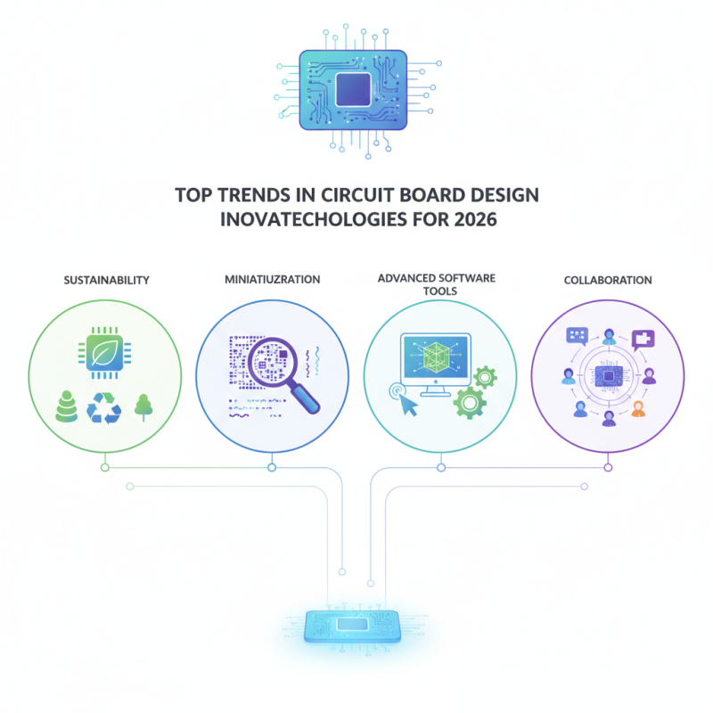
The world of circuit board design is evolving rapidly. Innovations in technology drive this transformation. As we approach 2026, several trends are emerging that highlight these changes. More companies focus on sustainability in their designs. Eco-friendly materials gain prominence in circuit board design. These materials reduce the carbon footprint.
Moreover, miniaturization remains a key theme. Devices are getting smaller, pushing designs to the limits. This challenge requires innovative solutions and careful engineering. Advanced software tools help designers simulate and test their ideas effectively. However, the pressure to meet tighter deadlines can lead to overlooked details.
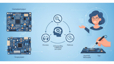
Collaboration is also changing circuit board design. Teams from various fields work together more than ever. This diversity can spark creativity but may also introduce misalignment. Designers must navigate these complexities to create effective products. The future holds exciting changes, but engineers must be ready to adapt and refine their strategies.
Emerging Materials and Their Impact on Circuit Board Design
The circuit board industry is witnessing a wave of innovation driven by emerging materials. These materials are redefining what’s possible in design and functionality. For instance, according to a recent report by the International Journal of Electronics, the use of advanced composites can increase thermal conductivity by up to 30%. This improvement is critical for managing heat in densely packed circuits.
Flexible materials are becoming increasingly popular. They enable circuits to be bent or twisted, making design more versatile. A study noted that flexible PCBs can reduce weight by approximately 50% compared to rigid boards. This reduction in weight is essential for portable devices. However, there are challenges. Manufacturers struggle with the durability of these materials. Some flexible PCBs have been reported to fail under high-stress conditions.
Moreover, the adoption of biodegradable materials is gaining momentum. Research shows that these materials could reduce e-waste significantly. However, they often lack the performance of traditional materials. Balancing environmental impact and performance remains a key issue for designers. Each emerging material presents its own set of strengths and weaknesses. Thus, continuous evaluation is necessary to optimize circuit board design.
Advancements in CAD Tools for Enhanced PCB Design Efficiency
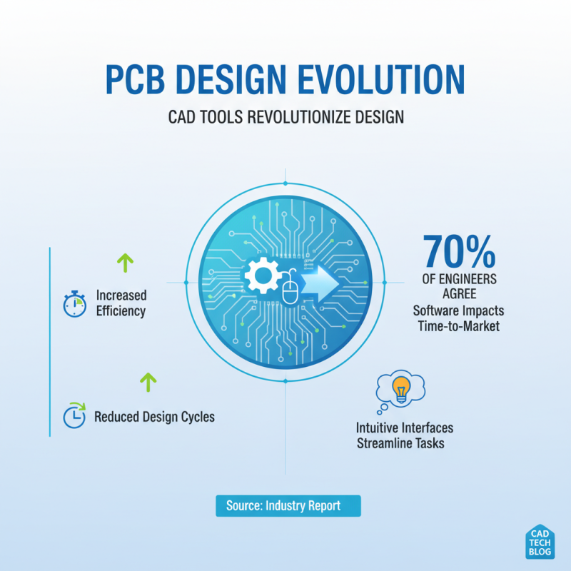
The field of PCB design is rapidly evolving, driven by advancements in CAD tools. These tools are enhancing efficiency and reducing design cycles. According to a recent industry report, 70% of engineers believe that improved software can significantly impact product time-to-market. They highlight the need for intuitive interfaces that streamline complex tasks.
Enhanced PCB design tools now incorporate artificial intelligence and machine learning algorithms. These technologies assist in automated error detection and optimization. A significant 65% of firms reported that these innovations reduced rework and costly errors. However, as technology advances, the skill gap among professionals may widen, leading to uneven adoption rates. Some designers find it challenging to keep up with the latest features and functionalities.
Moreover, many users express concerns about over-reliance on these tools. While they offer powerful capabilities, creativity and critical thinking remain essential. There are instances where designers overlook basic principles due to automation. Therefore, balancing technology and fundamental PCB knowledge is crucial for sustainable innovation in circuit board design.
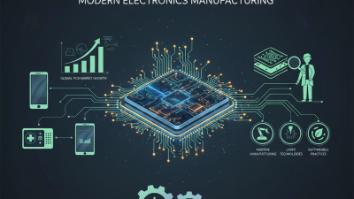
Integration of IoT Technologies in Modern Circuit Board Applications
The integration of IoT technologies in modern circuit board applications is transforming the electronics landscape. A recent report indicates that the global IoT market is expected to reach $1.1 trillion by 2026, highlighting the critical role circuit boards play in this growth. As devices become smarter, circuit boards must adapt to handle increased data processing demands.
Designers are focusing on compactness and efficiency. Innovations like multi-layer PCBs allow for high-density connections while maintaining performance. But with these advancements come challenges. The complexity of designs can lead to higher failure rates if not managed properly. Reports show that up to 30% of new designs may encounter issues during production.
Real-time data processing capabilities are now essential. Circuit boards must support various IoT protocols like MQTT and CoAP. However, ensuring compatibility and security can be daunting. As interconnected devices proliferate, manufacturers must prioritize robust security measures.
Look at emerging techniques such as AI-driven design tools that help identify potential flaws early. Embracing these technologies is crucial as it sets the foundation for future enhancements in circuit board applications.
Sustainability Practices in Circuit Board Manufacturing and Disposal
Sustainability in circuit board manufacturing is critical. The electronics industry generates approximately 50 million metric tons of e-waste annually. A significant portion of this waste is circuit boards. They contain hazardous materials that harm the environment and human health.
Recent studies show that adopting eco-friendly materials can reduce waste. For example, biodegradable substrates are gaining traction. These alternatives decrease the reliance on traditional materials like FR-4. However, the transition is not without challenges. Many manufacturers still prioritize cost over sustainability. This neglect can lead to long-term environmental repercussions.
Recycling practices are also evolving. Advanced techniques can recover up to 90% of valuable metals from discarded boards. Yet, only about 20% of e-waste is recycled today. Efforts must improve in the recycling sector to address this gap. Sustainable methods not only protect the environment but can also enhance brand reputation. The industry must take responsibility. Every innovation should keep sustainability at its core for a better future.
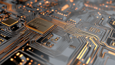
Trends in Miniaturization and Multi-layer PCB Architectures
In recent years, miniaturization has become a driving force in circuit board design. Engineers are challenged to create smaller, more efficient devices. Multi-layer PCB architectures play a crucial role in this trend. They allow for increased functionality without expanding the board's footprint. By stacking layers, designers can integrate more components in tighter spaces.
One important tip: focus on optimizing layer count. Reducing unnecessary layers can save space. However, this requires careful planning. Too few layers may limit functionality. On the other hand, too many can complicate the design. Balance is key.
Another aspect to consider is thermal management. As circuits become denser, heat generation increases. Implementing effective cooling solutions is vital. Not addressing heat can lead to failures. It’s essential to test your designs under real-world conditions, even if they seem perfect on paper. This focus on testing can reveal unexpected issues and lead to better designs.
2026 Top Trends in Circuit Board Design Innovations and Technologies
| Trend |
Description |
Impact on Design |
Technology Used |
| Miniaturization |
Reduction in board size while maintaining functionality. |
Enables compact designs for portable devices. |
Advanced materials and micro-etching technologies. |
| Multi-layer PCB Architecture |
Use of multiple layers to support complex circuitry. |
Increases design flexibility and routing options. |
Stacked die and embedded components technology. |
| Flexible PCBs |
Flexible materials allow unique shapes and foldable designs. |
Facilitates innovative product designs in wearables. |
Polyimide and other flexible substrates. |
| 3D Printing of PCBs |
Direct printing of circuit boards using 3D technology. |
Rapid prototyping and low-volume manufacturing efficiency. |
3D inkjet and laser technology. |
| Embedded Components |
Integration of active components directly into PCBs. |
Reduced size and improved performance. |
Advanced assembly technologies and materials. |