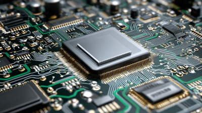
2025 Top Trends in Circuit Board Design: Innovations Shaping the Future
As we approach 2025, the landscape of circuit board design is set to undergo transformative changes driven by technological advancements and evolving market demands. According to the latest report by Research and Markets, the global printed circuit board market is expected to reach $88.48 billion by 2025, growing at a CAGR of 3.9%. This growth is fueled by the increasing integration of smart technologies in various sectors, including automotive, consumer electronics, and telecommunications, positioning circuit board design at the heart of innovation.

Dr. Emily Tran, a leading expert in electronic engineering and circuit board technology, emphasizes the importance of adaptability in this field: “The future of circuit board design lies in our ability to integrate artificial intelligence and flexible materials to create smarter, more efficient systems.” As design methodologies evolve to embrace more sustainable practices and advanced manufacturing techniques, engineers must stay ahead of the curve. The integration of emerging technologies such as 3D printing and IoT-enabled solutions will significantly influence how circuit boards are designed, fabricated, and implemented in the years to come.
The 2025 trends we will explore highlight key innovations that are not only shaping the circuit board design industry but also redefining the capabilities and applications of electronic devices across industries. Embracing these trends will be crucial for engineers and designers aiming to create cutting-edge solutions that meet the demands of a rapidly changing technological landscape.
Emerging Materials: The Shift to Flexible and Eco-Friendly Substrates in PCB Design
The shift towards flexible and eco-friendly substrates in PCB design is set to revolutionize the electronics manufacturing industry by 2025. As contemporary electronic devices produce considerable waste, adopting emerging materials can significantly minimize the environmental impact. Flexible substrates not only enhance the performance and usability of electronics but also promote a sustainable lifecycle, ensuring that products can be recycled or disposed of responsibly.
Incorporating innovative materials can lead to the development of hybrid sensor technologies optimized for sustainability. For instance, printed hybrid sensor tags for disposable healthcare and environmental monitoring applications are designed with both efficiency and ecological responsibility in mind. These advances allow businesses to meet consumer demand for greener products while also addressing regulatory pressures for sustainability.
**Tip 1**: Explore partnerships with startups that focus on sustainable materials in PCB design. Collaborating with innovators can provide unique insights and offerings that align with eco-friendly trends.
**Tip 2**: Implement a life cycle assessment approach in your business. This method can help identify areas where waste can be reduced, ultimately leading to more responsible production practices.
By embracing these trends, companies can enhance their products' market appeal and ensure a more sustainable future for electronics manufacturing.
2025 Top Trends in Circuit Board Design
Advancements in PCB Manufacturing: Embracing 3D Printing Technology for Prototyping
The advancement of 3D printing technology is set to revolutionize
PCB manufacturing, paving the way for innovative designs and rapid prototyping in circuit board development.
As industry leaders anticipate a thriving 3D printing market, projected to
reach $35.79 billion by 2030, the integration of this technology into
PCB prototyping offers manufacturers a new realm of opportunities. The ability to create complex geometries
and customized structures at a fraction of traditional production costs enhances design flexibility and
accelerates time-to-market for new electronic products.

Moreover, recent developments in micro-nano device manufacturing
through 3D printing have gained momentum, emphasizing the importance of precision
in circuit board applications. The incorporation of bio-microsystem integration
and Lab-on-PCB technology are creating sophisticated systems capable of
performing advanced functions in minimal space. As companies embrace these innovations, we can expect a shift
towards more sustainable and efficient
manufacturing practices in the PCB industry, ultimately leading to the creation of smarter,
more adaptable electronic solutions.
Integration of AI and Machine Learning in Circuit Board Design Optimization
The integration of artificial intelligence (AI) and machine learning (ML) is revolutionizing circuit board design, providing unprecedented optimization opportunities that enhance both performance and efficiency. By leveraging vast datasets, AI algorithms can predict and address design challenges earlier in the development process, ensuring optimal configurations that align with specific operational requirements. This capability allows designers to experiment with various layouts and materials, reducing the time-consuming iterations traditionally needed in creating circuit boards.
Moreover, machine learning contributes by continuously analyzing and learning from previous designs, leading to better decision-making in future projects. Advanced predictive analytics can also foresee potential issues such as signal integrity and thermal management, enabling engineers to proactively implement solutions. As a result, the convergence of AI and ML in circuit board design not only streamlines production but also drives innovation, paving the way for more compact, efficient, and powerful electronic devices in an ever-evolving technology landscape.
Miniaturization Trends: The Push for Smaller, High-Performance PCBs in Electronics
The electronics industry is experiencing a significant transformation, largely driven by the trend of miniaturization in printed circuit boards (PCBs). As demands for smaller, high-performance devices rise, the shift towards high-density interconnects (HDI) not only enhances device functionality but also improves efficiency and reliability across various sectors. Recent data highlights that the HDI PCB market is set to surpass USD 19.59 billion by 2025, propelled by innovations in miniaturization. This growth reflects the industry's commitment to delivering compact solutions that cater to modern consumer needs.
To adapt to these trends, companies should consider integrating advanced manufacturing technologies such as direct imaging systems, which accounted for more than 38.6% of the PCB market in 2024. This technology not only streamlines production but also reduces the footprint of electronic components, making way for creating smaller and more efficient devices.
**Tip:** When designing PCBs, prioritize the use of flexible printed circuit boards (FPCBs), projected to grow from USD 27.2 billion in 2025 to USD 98.1 billion by 2035. This shift not only supports the miniaturization movement but also opens new possibilities for complex circuit designs and enhanced performance in constrained spaces. Emphasizing these advanced materials will be crucial for staying competitive in a rapidly evolving market.
Enhanced Thermal Management Solutions: Addressing Heat Dissipation in Complex Circuit Boards
As we move towards 2025, enhanced thermal management solutions are becoming increasingly vital in circuit board design, especially as devices become more compact and performance-driven. The shift towards high-density interconnects (HDI) and multilayer boards can lead to significant heat generation, necessitating efficient heat dissipation strategies. According to a recent report by Research and Markets, the global thermal management market is expected to grow from $11.3 billion in 2021 to over $21.2 billion by 2026, underscoring the urgency of addressing heat-related challenges in modern electronics.
To combat these issues, innovative materials and techniques are being implemented. Advanced thermal interface materials (TIMs), such as phase change materials and metal-based composites, are enhancing heat spreading capabilities. Additionally, the integration of microchannels and vapor chambers in PCB designs is gaining traction, allowing for superior cooling efficiency. As per the International Electronics Manufacturing Initiative (iNEMI), adopting these advanced thermal management solutions could reduce thermal resistance by up to 30%, significantly extending the lifespan and reliability of electronic components. Embracing these innovations will be crucial for the future of circuit board design as industries seek to meet rising performance demands while ensuring durability.